




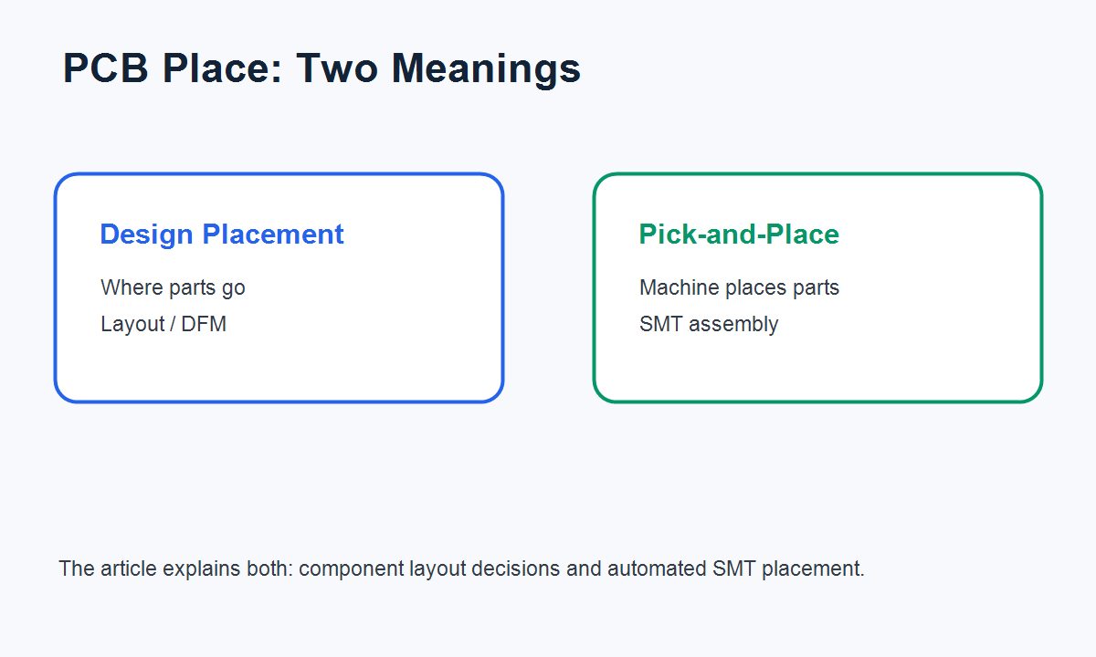
“PCB place” is not a precise standalone industry term, but buyers and engineers usually use it to mean one of two things: PCB component placement in the design layout, or SMT pick-and-place during PCB assembly. In both cases, it is about putting components in the right location, with the right orientation, so the board can be manufactured, inspected, tested, and used reliably.
If you are searching this term for a quotation or technical discussion, the clearer phrases are “PCB component placement,” “PCB layout placement,” or “PCB pick-and-place assembly.” This article explains both meanings and shows what engineers and procurement teams should check before ordering prototype or production PCB assembly.

PCB Place Usually Means Component Placement or Pick-and-Place
The safest way to understand 鈥淧CB place鈥?is to separate the design meaning from the assembly meaning. Design placement decides where each component sits in the PCB layout. Pick-and-place is the automated SMT process that mounts physical components onto solder paste during assembly.
| Term | What It Means | When It Applies | Buyer or Engineering Note |
| PCB component placement | Choosing where parts sit in the PCB layout | Design, DFM, routing, thermal planning | Review before Gerber and assembly files are released. |
| PCB layout placement | The EDA design stage before routing and manufacturing output | Hardware design and layout engineering | Critical parts, connectors, heat sources, and test points should be placed intentionally. |
| SMT pick-and-place | Machine placement of SMD components onto solder paste | PCB assembly production | Requires accurate BOM, CPL, rotation, polarity, and feeder setup. |
| CPL or centroid file | Coordinate file used by assembly equipment | SMT programming and placement setup | Incorrect rotation or side data can cause misplaced components. |
| DFA placement review | Assembly-focused review of component spacing and orientation | Prototype and production readiness | Helps reduce solder defects, rework, inspection difficulty, and yield loss. |
Good PCB Component Placement Starts with Function, Not Appearance
Component placement should begin with the circuit function, mechanical constraints, and manufacturing process. A board that looks neat can still fail if sensitive signals cross noisy power areas, heat sources are trapped, connectors do not fit the enclosure, or test points cannot be reached.
Designers usually place fixed mechanical parts first, such as connectors, mounting holes, switches, displays, antennas, sensors, and high-power devices. After that, they group components by function and keep critical paths short: power input to regulation, oscillator to IC, driver to load, connector to interface circuit, and decoupling capacitor to power pin.
Pick-and-Place Turns Digital Placement Data into Physical Assembly
In SMT assembly, pick-and-place machines use feeders, nozzles, cameras, and placement programs to mount components onto solder paste. The process depends on accurate design outputs, especially the BOM and CPL file.
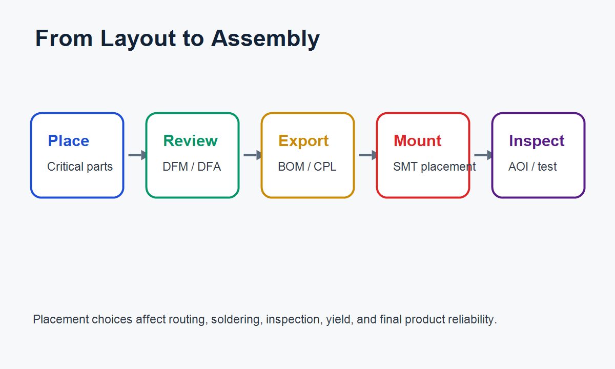
The CPL file lists component reference designators, coordinates, rotation, and board side. The BOM identifies the exact parts to load into feeders. The paste layer controls where solder paste is deposited. If these files do not agree with each other, the assembly line may stop for engineering confirmation or, worse, build a board with wrong orientation or wrong parts.
Placement Affects Routing, Signal Integrity, Heat, and Test Access
PCB placement is a major reliability decision because it controls how current, heat, signals, and technicians move through the board. Poor placement can make routing difficult, create EMI risk, increase voltage drop, hide test points, or place hot components too close to sensitive circuits.
- Signal integrity: keep high-speed paths short, controlled, and away from noisy switching areas where possible.
- Power integrity: place regulators, decoupling capacitors, and current paths to reduce loop area and voltage drop.
- Thermal control: keep hot parts away from heat-sensitive devices and allow copper, vias, airflow, or heatsinking when needed.
- Mechanical fit: match connectors, holes, buttons, displays, and keep-out areas to the enclosure and cable path.
- Testing: place test points where probes, fixtures, or technicians can access them without damaging nearby components.
Assembly-Friendly Placement Reduces Defects and Rework
Design for assembly is where component placement meets production reality. A placement that is electrically correct may still be difficult to solder, inspect, clean, rework, or test if the spacing and orientation are poor.
| Placement Issue | Manufacturing Risk | Practical Fix |
| Components too close together | Solder bridging, poor AOI visibility, difficult rework | Increase spacing around fine-pitch ICs, connectors, and polarized parts. |
| Unclear polarity orientation | Diodes, LEDs, capacitors, or ICs mounted incorrectly | Add clear silkscreen marks and confirm CPL rotation with the assembler. |
| Large parts near small passives | Shadowing, uneven heating, inspection difficulty | Review reflow and inspection access around tall components. |
| Poor fiducial placement | Machine alignment errors | Use clear board or panel fiducials according to the assembler’s process requirements. |
| Test points hidden under parts | Harder debug and production testing | Reserve accessible test points for power, ground, programming, and key signals. |
PCB Placement Files Must Match the BOM and Gerber Data
Most placement problems appear when file sets do not match. The board may have one footprint, the BOM may specify another package, and the CPL may contain rotation data that does not match the assembler’s machine convention.
- Gerber files: define copper, solder mask, paste, silkscreen, and board outline.
- BOM: identifies component values, part numbers, package types, quantities, and approved alternatives.
- CPL file: provides X-Y coordinates, rotation, board side, and reference designators.
- Assembly drawing: clarifies polarity, orientation, special handling, and mechanical notes.
- Test requirements: define what must pass before shipment.
Before production, the supplier should review file consistency and ask questions if component packages, rotations, or markings look unclear. For prototype builds, this review is especially valuable because early design data often changes quickly.
Cost and Lead Time Depend on Placement Complexity
PCB placement affects cost because it changes machine setup, assembly time, inspection effort, rework risk, and the number of process steps. A simple single-sided SMT board is usually easier to assemble than a dense double-sided board with BGAs, fine-pitch ICs, tall connectors, and mixed through-hole parts.
| Factor | Why It Matters | Buyer Check |
| Double-sided placement | May require extra reflow, adhesive, or process planning | Ask whether both sides can be assembled reliably with your component mix. |
| Fine-pitch components | Higher solder bridge and inspection risk | Confirm stencil design, AOI, and rework capability. |
| BGA or hidden joints | Requires stronger process control and sometimes X-ray inspection | Clarify inspection expectations before ordering. |
| Manual or through-hole parts | Can increase labor time and variability | Separate SMT and manual assembly requirements in the quotation request. |
| Unclear component alternatives | Sourcing delays and engineering approval loops | Provide approved substitutes when possible. |
Quality Checks Should Cover Placement Before and After Reflow
Reliable PCB assembly needs checks before soldering, during machine setup, and after reflow. Placement quality is not only about whether the component exists; it is about correct value, location, side, rotation, solder joint quality, and functional result.
- Pre-production file review: compare BOM, CPL, Gerber, paste layer, and assembly notes.
- First-article inspection: confirm part value, reference designator, orientation, and package match before continuing production.
- AOI inspection: check missing parts, offset parts, polarity, solder bridges, tombstoning, and visible solder defects.
- X-ray inspection: consider it for hidden solder joints such as BGA or bottom-terminated packages when required by the product risk.
- Electrical or functional testing: confirm that correct placement results in a working board, not only a visually acceptable board.
Supplier Selection Should Include Placement Review Capability
A strong PCB/PCBA supplier should be able to discuss placement risks before the build starts. This is especially important for custom products, prototypes, OEM projects, ODM support, and mass production where the same design must be repeatable.
- Ask whether the supplier performs DFM and DFA review before assembly.
- Confirm how they handle CPL rotation questions and polarity confirmation.
- Ask whether they can support prototype, sample development, and production scaling.
- Request inspection evidence that matches your product risk, not just generic quality wording.
- Confirm whether component sourcing, PCB fabrication, SMT assembly, testing, and packaging can be coordinated as one workflow.
For buyers sourcing from a China-owned source factory, the practical goal is not only a low unit price. The goal is a stable build package: clean files, manufacturable placement, clear communication, controlled assembly, and a supplier that can support the next revision or production stage.
Use This PCB Placement Checklist Before Ordering
A short placement checklist helps prevent avoidable assembly delays and first-build failures. Use it before sending files for quotation or before releasing a revised PCB layout.
- Confirm all footprints match the actual manufacturer part numbers.
- Check polarity markings for ICs, diodes, LEDs, electrolytic capacitors, connectors, and modules.
- Verify connector locations against the enclosure, cable direction, and user access.
- Keep hot components away from temperature-sensitive parts where possible.
- Keep decoupling capacitors close to IC power pins.
- Reserve access for programming, debugging, and production test points.
- Confirm high-speed, RF, or impedance-sensitive placement with the layout engineer.
- Check spacing around fine-pitch parts, BGAs, and tall components.
- Export a fresh BOM and CPL from the final layout revision.
- Ask the assembler to review CPL rotation before production if the package orientation is risky.
Frequently Asked Questions About PCB Place
What does PCB place mean?
PCB place usually refers to either component placement in PCB layout or the SMT pick-and-place process that mounts components onto a printed circuit board.
Is PCB place the same as pick-and-place?
Not always. Pick-and-place is the assembly machine process. PCB component placement can also mean the design decision of where components are located in the PCB layout.
Why is component placement important in PCB design?
Component placement affects routing, signal integrity, thermal performance, assembly yield, inspection access, testability, and long-term product reliability.
What files control PCB pick-and-place assembly?
A BOM, CPL or pick-and-place file, Gerber paste layer, assembly drawing, polarity notes, and approved component data are commonly used for SMT placement.
What is a CPL file in PCB assembly?
A CPL file, also called a centroid or pick-and-place file, lists component reference designators, X-Y coordinates, rotation, and board side for assembly machines.
What causes PCB placement errors?
Common causes include wrong footprints, incorrect rotation, unclear polarity, mismatched BOM data, poor fiducials, tight spacing, panelization changes, and incomplete assembly drawings.
How does placement affect PCB assembly cost?
Placement can affect cost through assembly time, special handling, rework risk, stencil complexity, component package difficulty, double-sided assembly, and inspection requirements.
What is DFM for PCB placement?
DFM for PCB placement checks whether component spacing, orientation, footprints, solder access, thermal relief, fiducials, and test points are practical for manufacturing.
What is DFA in PCB assembly?
DFA means design for assembly. It focuses on whether the board can be assembled efficiently and reliably with available equipment, component packages, and inspection methods.
How can I reduce PCB pick-and-place mistakes?
Use verified footprints, clear polarity marks, complete BOM data, correct CPL rotation, good fiducials, assembly drawings, DFM review, and first-article inspection before larger production.
Can a supplier fix poor PCB placement?
A supplier can flag risks and suggest changes, but layout placement decisions should be corrected in the design files before production whenever possible.
When should I ask for PCB placement review?
Ask for placement review before prototype assembly, before changing component packages, and before moving from prototype to mass production.
Final Takeaway
PCB place is best understood as the connection between design placement and assembly placement. Good placement makes the PCB easier to route, easier to assemble, easier to inspect, easier to test, and more reliable in the final product.
If you’re sourcing reliable PCB/PCBA manufacturing, including OEM, ODM, prototyping, mass production, or custom engineering solutions, reach out to our engineering team for technical support and a quote at [email protected].



0 Comments