




To solder PCB components, place the component correctly, heat the pad and lead together, feed solder to the heated joint, then remove the solder and iron so the joint cools without movement. A good solder joint should be smooth, shiny or evenly finished depending on solder alloy, shaped like a small cone or fillet, and free from bridges, cracks, excess solder, or lifted pads.
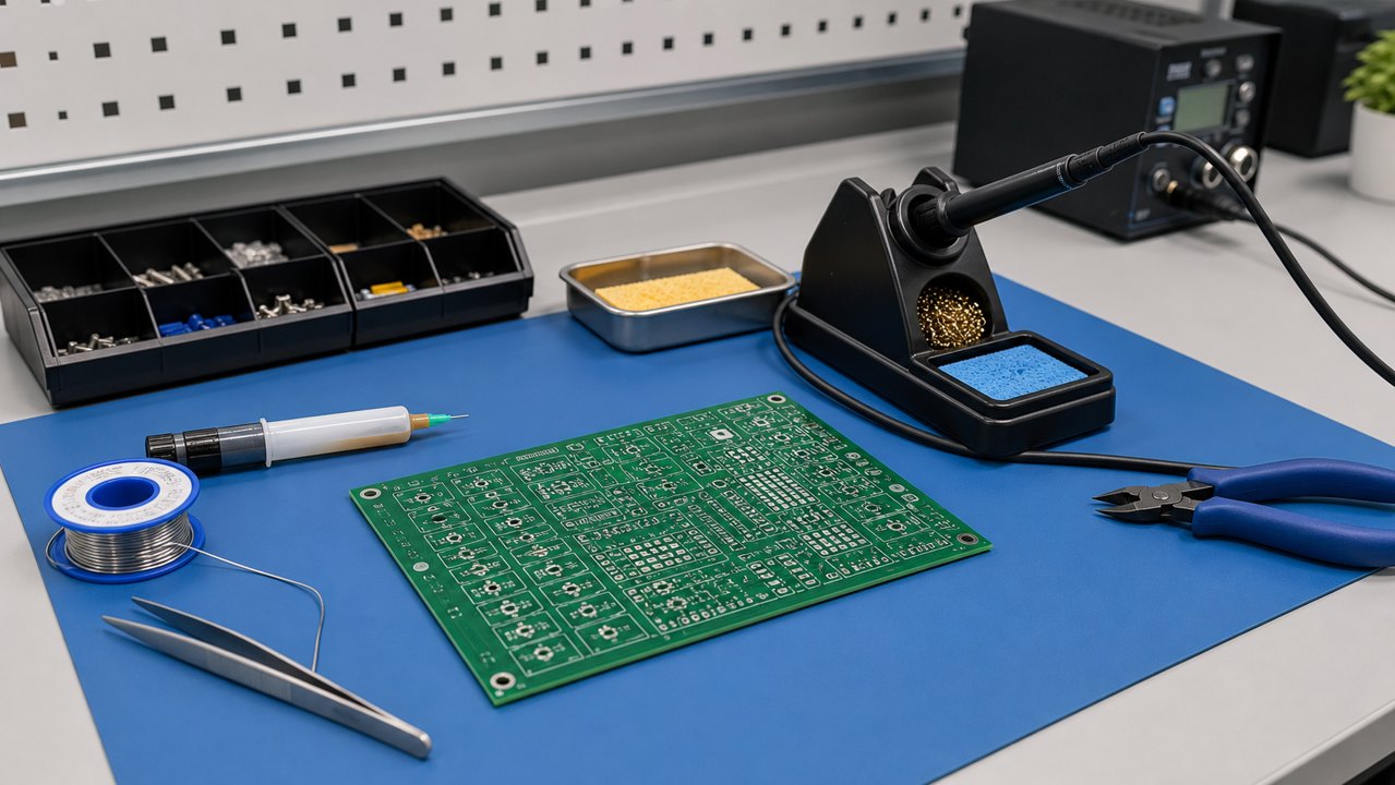
This guide focuses on how to solder PCB prototypes, small repairs, connector installation, and engineering validation. It also explains when hand soldering is not enough and when a professional PCBA process, stencil printing, reflow, AOI, or functional testing is the safer path.
Start With the Right PCB Soldering Tools
Good soldering is easier when the iron, solder, flux, and inspection tools match the PCB and component size.
For most PCB board soldering, use a temperature-controlled soldering station, a clean tip, fine solder wire, no-clean or rosin flux, tweezers, flush cutters, isopropyl alcohol when cleaning is required, and magnification for inspection. An ESD mat and wrist strap are recommended when handling sensitive ICs, MOSFETs, sensors, RF parts, or assembled boards.
| Tool or Material | Purpose | Buyer or Engineering Note |
| Temperature-controlled soldering iron | Provides stable heat for pads, leads, connectors, and repair work | A small conical or chisel tip is useful for common PCB joints |
| Solder wire | Forms the electrical and mechanical joint | Use a diameter that fits the joint size; fine wire gives better control |
| Flux | Improves wetting and helps solder flow onto copper and component leads | Extra flux is often the difference between a clean joint and a dull bridge |
| Tweezers and cutters | Hold parts, trim leads, and control small components | Use ESD-safe tweezers for sensitive parts |
| Magnifier or microscope | Checks fillets, bridges, cracks, and pad damage | Inspection is essential for fine-pitch and repair work |
| Fume extraction | Pulls flux fumes away from the operator | Use ventilation; do not breathe soldering fumes directly |
Prepare the PCB Board Before Soldering
A clean, stable board reduces cold joints, poor wetting, and accidental movement while the solder cools.
Check the PCB for contamination, oxidation, damaged pads, incorrect footprint orientation, missing solder mask clearance, and unclear polarity markings. If the board has been handled often, clean the area as appropriate for the flux and board finish. Secure the PCB with a holder so the board does not move when the soldering iron touches the joint.
Before applying heat, confirm component orientation. Diodes, LEDs, electrolytic capacitors, ICs, connectors, and polarized modules must match the silkscreen, assembly drawing, or schematic. Reversing a polarized component can damage the board during power-up even if the soldering itself looks clean.
Choose a Suitable Soldering Temperature
The best soldering temperature is high enough to heat the pad and lead quickly, but not so high that it burns flux, damages pads, or overheats components.
Exact settings depend on solder alloy, tip size, copper area, board thickness, and component thermal mass. Lead-free solder usually needs a higher tip temperature than tin-lead solder. Large ground pads, connectors, terminals, and thick copper boards may need more thermal capacity, while small pads and delicate components need careful control.
| Soldering Situation | Practical Temperature Logic | Risk to Watch |
| Small through-hole signal parts | Use moderate heat and short contact time | Cold joint if the pad and lead are not heated together |
| Lead-free solder | Often requires a higher iron setting than tin-lead solder | Burned flux or pad lifting if contact time is too long |
| Ground pins or connector shells | Need more heat transfer because copper planes pull heat away | Incomplete wetting around the barrel or pad |
| Fine-pitch SMD pins | Use flux, a clean fine tip, and minimal solder volume | Solder bridges and overheated pads |
How to Solder Through-Hole Components on a PCB Board
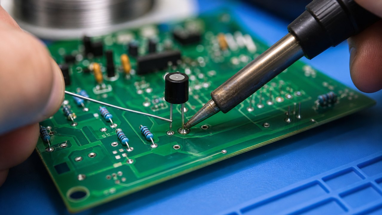
Through-hole soldering works best when the soldering iron heats the component lead and PCB pad at the same time.
- Insert the component into the correct holes and confirm polarity or orientation.
- Bend the leads slightly or use tape/fixture support if the part may fall out.
- Clean and tin the soldering iron tip with a small amount of solder.
- Place the tip so it touches both the pad and the component lead.
- Wait briefly for both surfaces to heat, then feed solder to the joint, not directly to the iron tip.
- Let solder flow around the lead and pad until it forms a smooth fillet.
- Remove the solder wire first, then remove the iron.
- Hold the part still while the joint cools.
- Trim the excess lead after the joint is solid, leaving enough lead length for reliability.
How to Solder Wires, Connectors, and Larger Pads
Wires and connectors need stronger mechanical support and often require more heat than small signal components.
Pre-tin stranded wires before inserting them into the PCB or connector pad. If the wire will move in service, add strain relief because solder is not a flexible mechanical joint. For large connector pins, ground tabs, terminals, or thick copper areas, use a tip with enough thermal mass rather than simply increasing temperature aggressively.
If solder does not flow, add flux and confirm the surfaces are clean. Do not keep pressing the iron against the pad for a long time. Excessive heat can lift pads, soften nearby plastic connectors, or damage plated through holes.
How to Hand Solder Small SMD Parts on a PCB
Small SMD parts can be hand soldered, but they require flux, good positioning, and careful solder volume.
For resistors and capacitors, tin one pad lightly, hold the part with tweezers, reheat the tinned pad to tack one side, then solder the other side. After the part is aligned, reflow the first side if needed. For small ICs, tack opposite corner pins first, then solder the remaining pins with flux and a small amount of solder. Solder wick can remove bridges if too much solder is applied.
Very fine-pitch ICs, QFN packages, BGA packages, thermal pads, and high-density assemblies are often better handled with stencil printing, controlled reflow, hot air, or professional PCBA equipment. Hand soldering may be useful for prototypes, but it is not always the right production process.
Inspect the Solder Joint Before Powering the Board
Inspection should happen before electrical power is applied because a solder bridge or reversed part can damage the circuit.
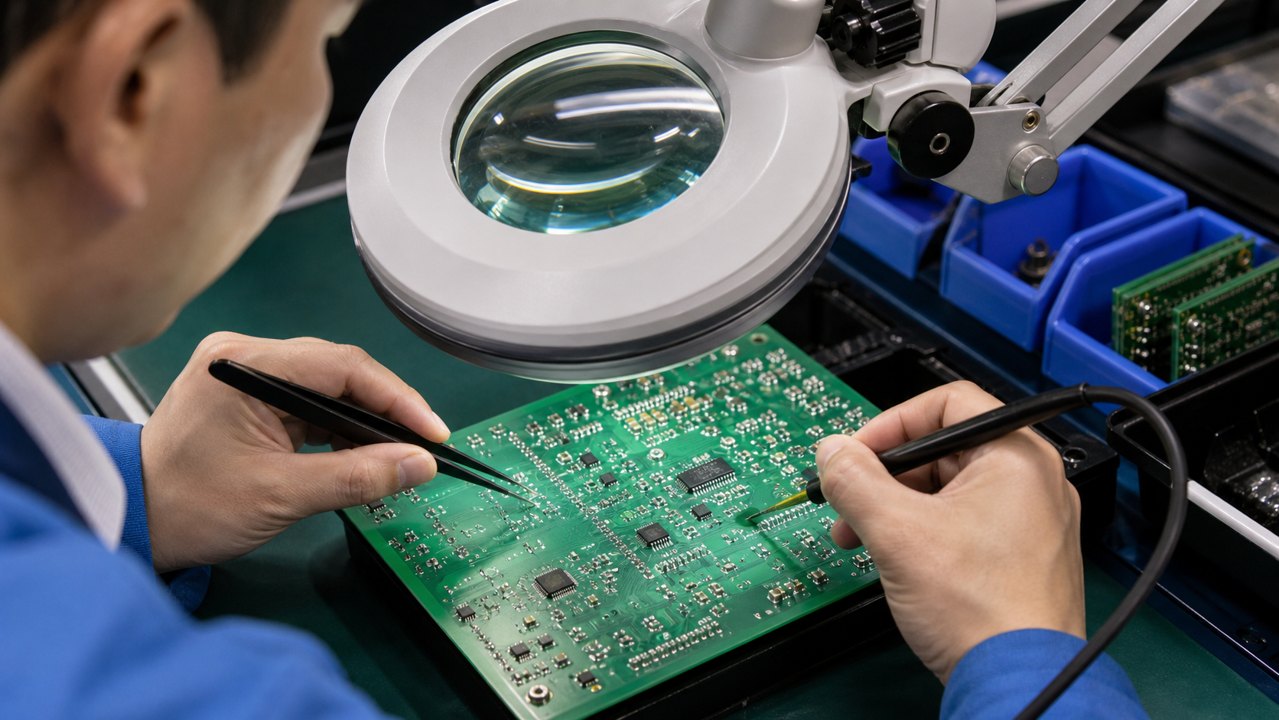
Use magnification and good lighting to check each joint. A good through-hole joint normally wets both the lead and pad, fills the barrel where appropriate, and has a clean fillet. A poor joint may look dull, cracked, balled up, bridged to a nearby pad, or barely attached to the component lead.
| Defect | What It Looks Like | Common Cause | Practical Fix |
| Cold joint | Dull, rough, cracked, or poorly wetted solder | Pad and lead were not heated enough or moved while cooling | Add flux and reflow until solder wets both surfaces |
| Solder bridge | Solder connects two adjacent pads or pins | Too much solder, insufficient flux, or fine pitch spacing | Use flux and solder wick to remove excess solder |
| Insufficient solder | Lead or pad is partly exposed and fillet is weak | Not enough solder or poor heat transfer | Reheat pad and lead, then add a small amount of solder |
| Excess solder | Large blob hides the pad shape or nearby clearance | Solder wire fed too long or too thick | Remove excess with solder wick and inspect again |
| Lifted pad | Pad separates from PCB laminate | Too much heat, pulling parts while solder is solid, or repeated rework | Stop rework and evaluate repair options before continuing |
Clean Flux Residue When the Process Requires It
Flux residue should be handled according to the flux type, board cleanliness requirement, and product application.
No-clean flux is often left in place when used correctly, but visible residue, sticky deposits, high-impedance circuits, RF circuits, conformal coating, and sensitive products may require cleaning. Use a cleaning method compatible with the flux, components, and PCB material. Do not soak parts that are not sealed or solvent-safe.
For production work, define the cleanliness requirement before assembly begins. Cleaning after the wrong flux or process choice can be slower and riskier than choosing the right soldering process from the start.
Test the PCB Board After Soldering
Testing confirms that solder joints are not only visually acceptable but also electrically functional.
Before powering the board, use a multimeter to check obvious shorts between power and ground rails. Verify polarity-sensitive components and connector orientation. For prototypes, power the board with current limiting when possible. For production or customer-ready assemblies, use defined inspection and test plans such as AOI, electrical test, in-circuit test, or functional test depending on the product.
- Check for solder bridges around fine-pitch pins and connector rows.
- Measure continuity where required and isolation where shorts would be dangerous.
- Confirm power rails before installing expensive modules or applying full load.
- Document any manual rework so later builds can improve the design or process.
Know When Hand Soldering Is Not the Best Choice
Hand soldering is useful for prototypes and repairs, but it is not always reliable for repeat production or dense assemblies.
If the PCB includes many SMD components, BGAs, thermal pads, tight-pitch ICs, controlled solder paste volume, or consistent production quality requirements, professional PCBA assembly is usually better. Stencil printing, pick-and-place, reflow profiling, AOI, X-ray for hidden joints, and controlled inspection reduce variation that hand soldering cannot always control.
For engineering teams, the practical decision is simple: use hand soldering for controlled prototype changes, connector additions, small repairs, and low-risk validation. Use professional assembly when repeatability, traceability, visual consistency, and quality control matter.
Design Tips That Make PCB Soldering Easier
Good PCB design makes soldering cleaner, faster, and less risky.
Designers can improve solderability by using correct pad sizes, clear polarity markings, suitable component spacing, thermal reliefs on large copper planes, readable silkscreen, and realistic footprints. For hand-soldered prototypes, extra spacing around connectors, test points, programming headers, and rework-prone parts can save time.
Useful design checks include:
- Confirm footprints against real component datasheets before ordering boards.
- Use thermal reliefs where large copper pours make pads difficult to heat.
- Add test points for important power, ground, programming, and signal nodes.
- Keep polarity marks visible after components are installed.
- Allow enough clearance for soldering iron access on prototype boards.
FAQ About How to Solder PCB
What is the basic method for soldering a PCB board?
Place the component, heat the pad and lead together, feed solder into the heated joint, remove the solder wire, remove the iron, and let the joint cool without movement. Then inspect for wetting, bridges, and component orientation.
Should solder be applied to the iron or the PCB joint?
Use a small amount of solder to tin the iron tip, but feed the main solder to the heated pad and lead. This helps the solder wet the actual joint instead of only melting on the iron tip.
Why does solder not stick to my PCB pad?
The pad may be dirty, oxidized, not hot enough, or lacking flux. Add suitable flux, clean the area if needed, and make sure the iron tip heats both the pad and component lead long enough for solder to flow.
What does a good PCB solder joint look like?
A good joint wets the pad and lead, has a smooth fillet, and does not form a ball, bridge, crack, or spike. Lead-free solder may look less shiny than tin-lead solder, so shape and wetting matter more than shine alone.
How do I fix a cold solder joint?
Add flux, reheat the joint until the solder flows properly, and add a small amount of fresh solder if needed. Keep the component still while the joint cools. If the pad is damaged, stop and assess repair options.
How do I remove a solder bridge on a PCB?
Apply flux and use solder wick or a clean iron tip to remove excess solder between pads or pins. After removing the bridge, inspect with magnification and check continuity if the circuit is sensitive.
Can I solder SMD components by hand?
Yes, many resistors, capacitors, small ICs, and connectors can be hand soldered with flux, tweezers, and magnification. Very fine-pitch parts, QFN packages, BGAs, and thermal pad parts are usually better assembled with controlled equipment.
Do I need flux for PCB soldering?
Flux is strongly recommended because it improves wetting and helps prevent dull joints and bridges. Many solder wires contain flux core, but extra flux is often helpful for rework, SMD parts, oxidized surfaces, and fine-pitch soldering.
Should I clean the PCB after soldering?
It depends on flux type and product requirements. No-clean flux may remain if used correctly, but visible residue, sensitive circuits, coating, RF work, or customer cleanliness requirements may need compatible cleaning.
What causes lifted pads during soldering?
Lifted pads are commonly caused by excessive heat, long contact time, repeated rework, or pulling components before solder is fully molten. Use proper temperature, flux, and gentle handling to reduce the risk.
Is hand soldering reliable for production PCB assembly?
Hand soldering can be reliable for selected through-hole parts, repairs, and low-volume work when controlled and inspected. For dense SMT production, professional assembly methods usually provide better repeatability and quality control.
What should I check before powering a freshly soldered PCB?
Check polarity, component orientation, solder bridges, cold joints, excess solder, power-to-ground shorts, and connector placement. Use current-limited power when possible for first power-up of a prototype.
Final Thoughts on PCB Board Soldering
Soldering in a PCB board is a practical skill, but reliable results come from controlled heat, clean surfaces, enough flux, correct component orientation, and careful inspection. For prototypes and repair, hand soldering is often useful. For dense assemblies or repeat production, a controlled PCBA process is usually safer and more consistent.
If you’re sourcing reliable PCB/PCBA manufacturing, including OEM, ODM, prototyping, mass production, or custom engineering solutions, reach out to our engineering team for technical support and a quote at [email protected].
Related PCB Guides
If you are using this guide to prepare a PCB project, these related PCBTRY guides can help you connect the next step instead of reading each topic in isolation.



0 Comments