




To make a Gerber file for PCB manufacturing, export every required copper, solder mask, silkscreen, paste, board outline, and drill file from your PCB design software, then check the package in an independent Gerber viewer before sending it to a manufacturer. The goal is not only to create files, but to make a package that a fabrication engineer can quote, panelize, drill, image, etch, inspect, and build without guessing.
What Is a Gerber File in PCB Manufacturing?
A Gerber file is a standard manufacturing output that tells a PCB fabricator what copper, solder mask, silkscreen, paste, and board-shape features should appear on each layer. In most projects, Gerbers are submitted together with drill files, a board outline, a stackup note, and key fabrication requirements.
If you need a deeper background on the format itself, PCBTRY already has a guide to Gerber files for PCB manufacturing. This article focuses on the practical export and pre-quote checks that reduce delays after the design is finished.
Which Files Should You Export?
A complete PCB fabrication package usually needs Gerber layers plus drill and documentation files, not only one copper image. Missing drill, outline, or stackup information is a common reason a quote is delayed.
| File or layer | What it controls | What to check |
| Top and bottom copper | Traces, pads, planes, and copper pours | Layer polarity, clearances, and missing pours |
| Inner copper layers | Power planes, signal layers, and impedance structures | Layer order and stackup match |
| Solder mask | Mask openings around pads and exposed copper | Mask expansion and solder bridge risk |
| Silkscreen | Reference designators, polarity marks, and labels | Text on pads, unreadable labels, wrong orientation |
| Paste layer | Stencil openings for SMT assembly | Only needed when assembly or stencil data is required |
| Drill file | Hole position, tool size, plated or non-plated holes | Units, zero suppression, slots, and tool table |
| Board outline | Final shape, cutouts, and routed features | Closed outline and mechanical layer consistency |
| Readme or fabrication note | Thickness, copper weight, finish, color, tolerance, stackup | No conflict with exported layer count |
How to Export Gerber Files from PCB Design Software
The exact menu changes by tool, but the manufacturing logic is the same: select the right layers, use consistent units, export drill data, and confirm the output in a viewer. Do not assume the design software preview and the exported Gerber package are identical.
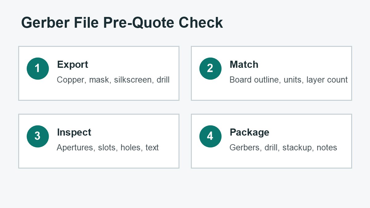
- Open the completed PCB layout and run the electrical rule check and design rule check.
- Open the fabrication output, CAM processor, or plot/export menu.
- Select all copper layers, solder mask, silkscreen, paste layers if needed, and the mechanical board outline layer.
- Use RS-274X / extended Gerber unless your manufacturer asks for another format.
- Export Excellon drill data with the same unit system used by the Gerbers.
- Export the pick-and-place file and BOM separately if PCBA assembly is part of the order.
- Zip the Gerbers, drill files, stackup note, and fabrication requirements into one package.
Before export, review common PCB layout checks such as clearance, board edge spacing, reference marks, and mechanical fit. A clean layout makes the Gerber export much less risky.
What Should You Check in a Gerber Viewer?
You should check the exported files in an independent Gerber viewer because it shows what the manufacturer will receive, not what your design editor intended. This catches missing layers, wrong units, shifted drill holes, and outline mistakes before the package reaches quoting.
- Confirm the board outline is visible, closed, and aligned with the copper.
- Turn layers on and off to check top, bottom, and inner copper order.
- Overlay drill data and confirm holes sit in pads, not beside them.
- Check plated and non-plated holes, slots, and cutouts.
- Look for silkscreen text crossing pads or polarity marks hidden by components.
- Confirm solder mask openings expose only the intended pads.
- Compare the viewer layer count with the stackup note.
How Do Gerber Files Affect PCB Quotes?
Gerber files affect PCB quotes because they reveal the real board size, layer count, hole structure, copper area, minimum spacing, surface finish needs, and manufacturability risk. A vague screenshot or incomplete export can make the price slower or less accurate.
For example, a quote engineer may need to know whether small holes are plated vias, whether slots need routing, whether the layer count matches the stackup, and whether fine traces require a tighter fabrication process. A practical DFM review before fabrication is often the fastest way to catch these issues.
Common Gerber Export Mistakes
Most Gerber problems are not complex engineering failures; they are small packaging errors that make the manufacturer stop and ask for clarification. The earlier you catch them, the less time you lose during quotation and engineering review.
- Drill file uses a different unit or zero-suppression setting from the Gerbers.
- Board outline is missing, open, or placed on an unclear mechanical layer.
- Inner layers are exported but not named clearly enough to show layer order.
- Solder mask openings are too large or missing on key pads.
- Silkscreen text overlaps exposed copper or assembly pads.
- Copper pours are not repoured before export.
- Fabrication notes conflict with the actual files, such as a 4-layer note with 2-layer Gerbers.
What Should You Send with Gerber Files?
Send enough context for the manufacturer to quote and build the board without guessing. Gerbers show geometry, but the factory still needs requirements such as thickness, copper weight, surface finish, solder mask color, material, tolerance, and special process notes.
| Item | Why it helps |
| Gerber files | Define visible manufacturing layers. |
| Drill files | Define hole sizes, locations, and drill tools. |
| Stackup or layer order note | Prevents confusion on 4-layer, 6-layer, HDI, and impedance boards. |
| Fabrication requirements | States thickness, copper weight, material, finish, mask color, and tolerance. |
| BOM and pick-and-place | Needed only when assembly quotation is required. |
| Special notes | Calls out controlled impedance, panel constraints, slots, press-fit holes, or edge plating. |
If you are unsure which manufacturing process your files imply, compare them with common PCB manufacturing techniques before sending the quote request.
Can a PCB Manufacturer Fix Gerber Problems?
A manufacturer can often flag Gerber problems and suggest corrections, but they should not silently guess design intent. The safest workflow is to let the factory report manufacturability concerns while the designer approves any geometry, layer, or drill change.
Simple issues such as unclear notes or missing fabrication details may be fixed through communication. Design-impacting issues such as pad size, trace clearance, layer order, controlled impedance, or drill definition should be corrected in the source CAD project and re-exported.
Pre-Quote Checklist Before Sending Gerbers
A short checklist prevents most Gerber-file delays before a quote request is submitted. Use it before every prototype or production order, especially when the board has multiple layers, slots, dense components, or impedance requirements.
- All required copper, mask, silkscreen, paste, drill, and outline files are included.
- Gerbers and drill data open correctly in an independent viewer.
- Layer names clearly show top, bottom, and inner-layer order.
- Board outline aligns with copper and drill data.
- Fabrication notes match the exported layer count and board size.
- Minimum trace, spacing, hole, annular ring, and solder mask bridge are realistic for the selected manufacturer.
- Special requirements such as impedance, HDI, castellated holes, slots, or edge plating are stated separately.
Questions to Ask Your PCB Manufacturer
Good supplier questions turn Gerber review from a file upload into a manufacturing check. They help you find unclear data before fabrication starts.
- Do the Gerbers, drill files, and stackup note match?
- Are any holes, slots, or cutouts unclear?
- Do any trace, spacing, solder mask, or annular ring values need DFM review?
- Is the board outline ready for routing or does it need mechanical clarification?
- Are there controlled impedance, material, or surface finish notes missing from the package?
- If assembly is required, do the BOM and pick-and-place file match the PCB revision?
FAQ
What format should Gerber files use?
Most modern PCB manufacturers accept RS-274X / extended Gerber files. Some projects may also use ODB++ or IPC-2581, but Gerber plus Excellon drill files remains a common starting point for PCB fabrication quotes.
Do I need a drill file with Gerbers?
Yes. Gerbers show layer artwork, but the drill file defines hole locations, tool sizes, and plated or non-plated features. Without drill data, the manufacturer cannot fully evaluate vias, mounting holes, slots, or through-hole components.
Should I send source CAD files instead of Gerbers?
Send Gerbers for fabrication unless your manufacturer specifically asks for source CAD files. Source files may expose editable design data, while Gerbers are controlled manufacturing outputs. For engineering support, source files can be shared separately when appropriate.
Why do Gerber files look different from the PCB design screen?
The PCB design screen may show components, design objects, or visual aids that are not part of manufacturing output. A Gerber viewer shows the exported fabrication layers, so it is the better reference for checking what the factory will receive.
Can I get a PCB quote with incomplete Gerber files?
You may get a rough discussion, but not a reliable manufacturing quote. Missing drill files, outline data, stackup notes, or fabrication requirements can change cost, lead time, and process feasibility.
Final Advice Before You Send Files
Making a Gerber file for PCB manufacturing is mainly about controlled export and verification. Export the correct layers, include drill and outline data, check everything in a separate viewer, and send clear fabrication notes with the package.
If you need a manufacturer to review your Gerber package before fabrication, contact PCBTRY’s PCB prototype and fabrication manufacturer team with your Gerbers, drill files, stackup, and board requirements for engineering feedback and a quote at [email protected].
Related PCB Guides
If you are using this guide to prepare a PCB project, these related PCBTRY guides can help you connect the next step instead of reading each topic in isolation.



1 Comment
Rigid-Flex PCB Manufacturing Process: Controls and Tests - thindry pcb manufacturer · 08/24/2026 at 17:03
[…] drawing and copper data disagree, manufacturing cannot safely infer the intended geometry. Review how to prepare Gerber files for PCB manufacturing before […]