




Anyone who has looked at a PCB drawing has probably noticed three types of vias mentioned again and again: through-holes, blind holes, and buried holes. They sound similar, but each one plays a different role in how a board connects, holds together, and performs under load. Understanding the difference matters when you’re deciding how a multilayer board should be built.
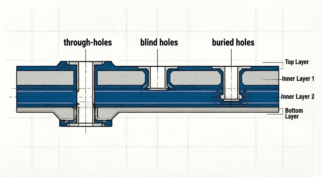
Through-Holes: The Backbone of the Board
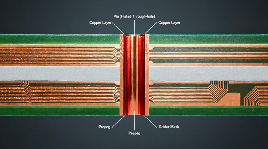
A through-hole runs from the top layer all the way to the bottom layer, passing through every layer in between. It’s the oldest and most common via type, and it still shows up in almost every design, even the most advanced ones.
Its main jobs are:
- Electrical connection across all layers, letting signals or power travel from one side of the board to the other
- Mechanical support, especially for component leads that get soldered directly into the hole
- Heat dissipation, since a plated through-hole can act as a thermal path away from hot components
- Structural rigidity, helping hold multilayer stacks together during lamination and drilling
Because it goes straight through the board, a through-hole is also the easiest and cheapest type to drill and plate. That’s part of why it remains the default choice unless there’s a specific reason to use something else.
Case Study: Through-Holes in Industrial Control Boards
On a typical four-layer industrial control board, power modules and high-current components are usually connected straight to the inner power and ground planes through plated through-holes. This approach has two clear advantages: through-holes offer low resistance and strong current-carrying capacity, which suits high-current paths, and they provide solid mechanical anchoring for component leads, reducing the risk of solder joint fatigue in environments with vibration. Components like relays and high-power MOSFETs are almost always mounted using through-holes for exactly this reason.
Blind Holes: Connecting the Surface to an Inner Layer
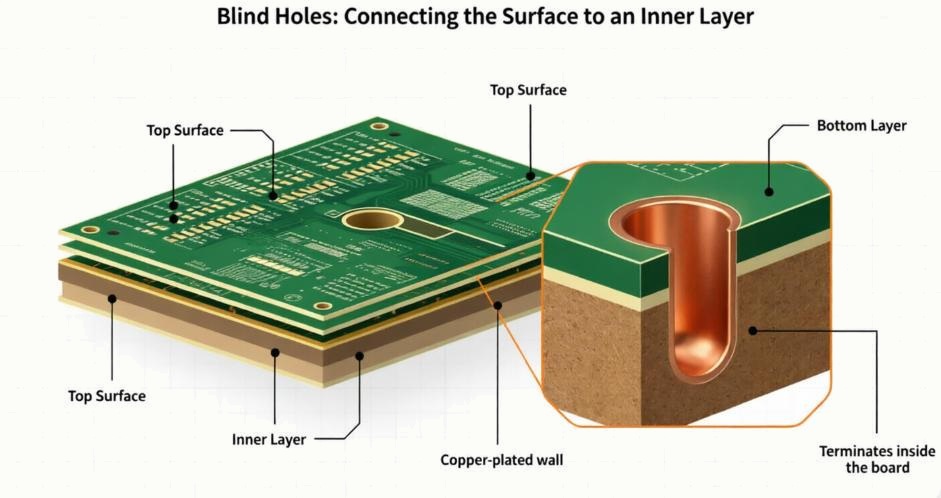
A blind hole starts from either the top or bottom surface but stops at an inner layer instead of going all the way through. It’s “blind” because you can only see it from one side.
Blind holes are used when a design needs to connect an outer layer to a specific inner layer without wasting space on layers that don’t need the connection. This is especially useful in dense boards where routing space is tight and every extra via that isn’t needed just gets in the way.
Typical reasons to use a blind hole include:
- Freeing up routing space on layers that don’t need that particular connection
- Supporting high-density interconnect (HDI) designs where components are packed closely together
- Reducing the overall via count needed for a specific signal path
The tradeoff is manufacturing complexity. Blind holes usually require controlled-depth drilling or laser drilling, along with more careful process control, which adds cost compared to a standard through-hole.
Case Study: Blind Holes in Smartphone Mainboards
Smartphone mainboards are one of the clearest examples of blind hole usage. Internal space is extremely limited, yet the board has to fit a processor, memory, RF modules, and power management chips, all packed into a tight routing area. If every connection relied on through-holes, there simply wouldn’t be enough room left for signal traces.
Engineers typically use laser-drilled blind holes to connect BGA pads on the top layer directly down to the second or third layer, without punching all the way through the board. This frees up the middle and bottom layers for other signal routing and allows the board to be made thinner and more compact. Many smartphone mainboards use stacked or sequential blind holes across multiple build-up layers, which is one of the core techniques behind HDI manufacturing.
Buried Holes: Hidden Inside the Layer Stack
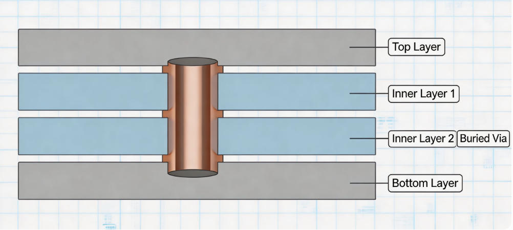
A buried hole connects two or more inner layers without reaching either outer surface. Once the board is fully laminated, there’s no way to see it from outside at all — it’s completely enclosed within the stack.
Buried holes are typically used in:
- High layer-count boards where inner-layer routing needs its own dedicated connections
- Designs aiming to reduce the number of through-holes taking up outer layer space
- Applications where signal integrity benefits from shorter, more direct inner-layer connections
Because buried holes have to be drilled and plated before the rest of the layers are laminated on top, they add extra process steps and require very precise layer alignment. This makes them the most expensive and technically demanding of the three via types.
Case Study: Buried Holes in Server Motherboards
Server and networking motherboards often run into the double digits in layer count, sometimes twenty layers or more, carrying a large volume of high-speed signals such as DDR memory buses and PCIe channels. These signals are sensitive to trace length and impedance consistency, and any unnecessary via can introduce reflections or crosstalk that degrade signal integrity.
Designers commonly use buried holes to connect certain inner signal layers directly, without routing out to an outer layer and back. This shortens the signal path and keeps the outer layers free of excess vias, leaving more room for thermal management and additional routing. This is also why high-speed, high layer-count server boards typically combine through-holes, blind holes, and buried holes all in the same design.
Comparing the Three
| Via Type | Connects | Visible From Outside | Typical Use Case | Relative Cost |
|---|---|---|---|---|
| Through-hole | Top to bottom, all layers | Both sides | General connections, component mounting, thermal paths | Lowest |
| Blind hole | Outer layer to inner layer | One side only | HDI designs, dense routing | Medium |
| Buried hole | Inner layer to inner layer | Not visible | High layer-count boards, inner routing | Highest |
Choosing the Right Combination
Most real-world boards don’t rely on just one via type. A design might use through-holes for component mounting and power delivery, blind holes to save space near a dense component area, and buried holes to keep certain inner-layer signals clean and short. The right mix depends on layer count, signal requirements, thermal needs, and budget.
Getting this combination right at the design stage saves a lot of trouble later. A board with unnecessary blind or buried holes ends up costing more to manufacture without any real benefit, while a board that needed them but used only through-holes might run into space or signal integrity problems.
If you’re working on a board and aren’t sure which via structure fits your design, it’s worth going over the layer stack-up and signal requirements with your manufacturing partner before finalizing the layout. Catching these decisions early usually means fewer revisions and a smoother path from design to production.
FAQ
1. Are blind holes and buried holes always better than through-holes?
No. Blind holes and buried holes solve space and signal problems, but they cost more, take longer to manufacture, and are more complex to produce. If a board has a low layer count and enough routing space, through-holes work perfectly well. There’s no need to add blind or buried holes just to make a design look more advanced.
2. Do blind holes and buried holes affect board reliability?
When designed and manufactured correctly, blind holes and buried holes are just as reliable as through-holes. However, they demand tighter control over drilling depth, layer alignment, and plating uniformity. If the process isn’t well controlled, issues like copper cracking or poor connections become more likely. Working with a manufacturer experienced in HDI processes matters a lot here.
3. When is it necessary to use blind or buried holes instead of just through-holes?
Two situations usually call for it. First, when component spacing is extremely tight, such as with high-density BGA packages, where standard through-hole diameters and clearances simply won’t fit. Second, when high-speed signals have strict requirements on trace length and impedance, where extra through-hole vias would introduce unacceptable signal loss. In both cases, through-holes alone aren’t enough.
4. How much do blind holes and buried holes add to the cost?
This varies quite a bit depending on layer count, whether the blind holes are stacked or sequential, and overall board thickness. As a general rule, a standard through-hole board sets the cost baseline, adding blind holes raises that cost noticeably, and adding multi-stage blind holes or buried holes pushes it higher still. It’s best to discuss your specific stack-up with your manufacturer for an accurate quote rather than estimating based on via type alone.
5. What’s the relationship between through-hole diameter and board thickness?
There’s a concept called aspect ratio, the relationship between hole diameter and board thickness, generally kept around 1:8 to 1:10 depending on manufacturing capability. Thicker boards with smaller holes make drilling and plating more difficult, and it becomes harder to maintain even copper plating along the hole wall. If your board is on the thicker side, avoid designing hole diameters too small, or you risk manufacturing issues.
6. Can a single board use through-holes, blind holes, and buried holes at the same time?
Absolutely, and it’s quite common in mid-to-high layer count, high-density designs. The server motherboard example above is a typical case. Designers usually choose the most suitable via type for each section of the board based on its specific connection needs, rather than using one via type across the entire board.
7. At what stage of design should via types be decided?
As early as possible. Via type selection is closely tied to the layer stack-up, impedance control, and component placement. Waiting until routing is nearly done to discover that space constraints require blind holes leads to costly rework. It’s best to lock in the via strategy during stack-up planning and critical signal routing decisions.
Most real-world boards don’t rely on just one via type. A design might use through-holes for component mounting and power delivery, blind holes to save space near a dense component area, and buried holes to keep certain inner-layer signals clean and short. The right mix depends on layer count, signal requirements, thermal needs, and budget.
Getting this combination right at the design stage saves a lot of trouble later. A board with unnecessary blind or buried holes ends up costing more to manufacture without any real benefit, while a board that needed them but used only through-holes might run into space or signal integrity problems.
If you’re working on a board and aren’t sure which via structure fits your design, it’s worth going over the layer stack-up and signal requirements with your manufacturing partner before finalizing the layout. Catching these decisions early usually means fewer revisions and a smoother path from design to production.
Frequently Asked Questions
1. Are blind holes and buried holes always better than through-holes?
No. Blind holes and buried holes solve space and signal problems, but they come with higher cost, more complex processing, and longer lead times. If a board doesn’t have many layers and routing space isn’t tight, through-holes work perfectly well. There’s no need to add blind or buried holes just to make a design look more advanced.
2. Do blind holes and buried holes affect board reliability?
When designed and manufactured correctly, blind and buried holes are just as reliable as through-holes. However, compared to through-holes, they demand tighter control over drill depth, layer-to-layer alignment, and plating uniformity. If the process isn’t well controlled, issues like copper cracking or poor connections become more likely. This is why working with a manufacturer experienced in HDI processes matters.
3. When is it actually necessary to use blind or buried holes instead of through-holes?
Two situations usually call for it. First, when component spacing is extremely tight, such as with high-density BGA packages, where standard through-hole diameters and spacing simply won’t fit. Second, when high-speed signals have strict requirements for trace length and impedance, where extra through-hole vias would introduce unacceptable signal loss. In both cases, through-holes alone can’t meet the design requirements.
4. How much extra cost do blind and buried holes add?
This varies quite a bit depending on layer count, via order (whether it’s a single or stacked blind hole), and board thickness. Generally, a standard through-hole board has the lowest cost baseline. Adding blind holes raises the cost noticeably, and adding stacked blind holes or buried holes on top of that increases it further. It’s best to discuss your specific stack-up with your manufacturer rather than pricing based on via type alone.
5. What’s the relationship between through-hole diameter and board thickness?
There’s a concept called aspect ratio, the relationship between hole diameter and board thickness, generally recommended to stay around 1:8 to 1:10 depending on the manufacturer’s process capability. Thicker boards with smaller holes are harder to drill and plate evenly, and copper plating on the hole wall becomes less consistent. If your board is on the thicker side, avoid designing holes that are too small, as it introduces manufacturing risk.
6. Can a single board use through-holes, blind holes, and buried holes all at once?
Yes, and this is actually common in mid-to-high layer count, high-density designs. The server motherboard example above is a typical case. Designers usually choose the most suitable via type for each section of the board based on its specific connection needs, rather than using one via type across the entire board.
7. At what stage of design should via type decisions be made?
As early as possible. Via type selection is closely tied to the layer stack-up, impedance control, and component placement. If routing is nearly finished before someone realizes there isn’t enough space and blind holes are needed, the rework cost can be significant. It’s best to lock in the via strategy during the stack-up planning and key signal routing stage.



0 Comments