




You power up a board and nothing happens — or worse, something smells like it’s burning. You pull the input fuse and it’s blown. You swap it, try again, and it blows again in under a second. At that point, you’re not debugging a firmware bug or a wrong component value. You have a short circuit somewhere on that board, and until you find it, nothing else matters.
Short circuits on PCBs kill components, waste production time, and — in high-current or high-voltage applications — create genuine safety hazards. The frustrating part is that they don’t always announce themselves with a burn mark. Many shorts are invisible to the naked eye: a whisker-thin solder bridge between two 0.3mm pitch pads, a tin whisker buried under a shield can, or a delaminated inner layer nobody can see without X-ray equipment.
We’ve been manufacturing and testing PCBs for over a decade. The methods below are what actually work, ordered roughly from “grab a magnifier” to “send it to the lab.” Which one you reach for first depends on your equipment, your time, and how complex the board is.
What Causes a Short Circuit on a PCB?
Before you start probing, it helps to know what you’re looking for. Most PCB shorts trace back to one of these root causes:
- Solder bridging — The most common cause on assembled boards. Excess solder flows between adjacent pads during reflow or wave soldering, creating a low-resistance path. Fine-pitch components (QFPs, BGAs,0.4 mm pitch connectors) are most susceptible.
- Tin whiskers — Spontaneous filament-like growths from tin or tin-alloy plating, most often seen on RoHS-compliant finishes. They grow slowly and can short adjacent pins weeks or months after assembly.
- Failed components — A shorted MOSFET, capacitor, or ESD diode can read as a board-level short. The component itself is the short — removing it clears the fault.
- Contamination — Flux residue, moisture, or conductive particulates can form resistive-to-dead short paths, especially on high-impedance nodes. This is common on boards that weren’t cleaned after soldering or were exposed to humid storage.
- Design rule violations — Inadequate trace-to-trace spacing, missing solder mask between pads, or undersized annular rings can create marginal gaps that become shorts under thermal or mechanical stress.
- Manufacturing defects — Etch residue left between copper features, layer misregistration causing internal via-to-trace contact, or lamination voids in multilayer boards. These are harder to find because they’re inside the stackup.
Knowing the likely cause narrows your search. A hand-soldered prototype with a fresh short almost certainly has a solder bridge. A production board that passed testing but failed in the field needs a different approach entirely.
Warning Signs You’re Dealing with a Short
Some of these are obvious. Others get misdiagnosed for too long:
- Board won’t power on, or immediately trips the power supply’s current limit
- Input fuse blows on first power-up (or repeatedly)
- Abnormally high current draw the moment power is applied — before the firmware even boots
- Localized heating on one section of the board within seconds of power-on
- Burning smell, discolored PCB surface, or visibly damaged components
- Battery drains rapidly even when the device appears to be idle
If you’re seeing any of these, stop powering the board and start with a cold inspection. Repeatedly forcing current through a short destroys evidence and can escalate damage.
How to Detect a Short Circuit on a PCB: 7 Methods
Method 1: Visual Inspection
Start here. It’s free, it’s fast, and for hand-soldered or prototype boards, it catches the majority of shorts.
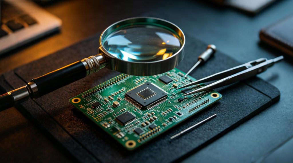
Use a magnifier — at minimum a 10× loupe, better still a stereo microscope at 20–40×. Work under bright, angled light so solder bridges catch the reflection differently from normal joints. Go systematically: start at the power input, follow the power planes, then check every fine-pitch component.
What you’re looking for:
- A thin solder bridge spanning two adjacent pads (sometimes barely visible as a slight “fullness” between pins)
- Burn marks or discoloration on traces, pads, or component bodies
- Foreign conductive material: metal shavings, dropped component legs, stray wire strands
- Lifted or peeled solder mask exposing adjacent copper features
Visual inspection won’t find inner layer shorts, tin whiskers under shields, or contamination beneath components. Don’t assume a clean visual means no short — use it to rule out the obvious before moving on.
Method 2: Multimeter Continuity / Resistance Test
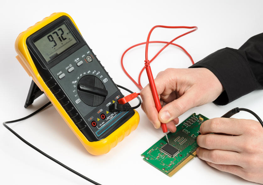
This is the most universally accessible electrical test. Every technician has a multimeter; this works on any board with the power off.
What you need: Digital multimeter with continuity or resistance mode.
Steps:
- Disconnect all power and discharge any bulk capacitors (wait at least 30 seconds for high-cap designs).
- Pull up the schematic. Identify the power net you suspect (VCC, 3V3, 5V, etc.).
- Set the meter to resistance mode (Ω). Measure between VCC and GND. A healthy board will read hundreds of ohms to megaohms depending on the design; a short reads under 10Ω, often close to zero.
- If you get a suspiciously low reading, switch to continuity mode. Systematically probe between power and ground at different points on the board to see if the reading changes — this can help triangulate the fault to a specific region.
- If you have a schematic and netlist, also test between nets that should have no connection. Any reading under ~1 MΩ between isolated nets warrants investigation.
Limitation: Components with low impedance between rails (bulk capacitors, ferrite beads, power ICs) can create misleading readings. When in doubt, desolder the suspected component and retest the board.
Method 3: Diode Mode Test
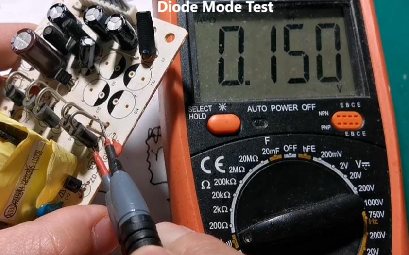
When the short appears to be through a semiconductor junction, switch your multimeter to diode mode. This lets you check the directionality of the path.
A healthy diode or ESD protection device will show a forward voltage drop of roughly 0.3–0.7 V in one direction and “OL” (open) in the other. If you read a near-zero voltage in both directions, the device has internally shorted. If you read a consistent ~0.6 V short between power and ground, there’s likely a protection diode conducting in a direction it shouldn’t be — which points to either a failed component or reversed polarity somewhere upstream.
This method is particularly useful on boards where the short is intermittent or low-resistance rather than a dead zero-ohm path.
Method 4: Power-On Current Monitoring
This is a non-destructive way to confirm a short is present and get a rough sense of its severity before you start probing with test leads.
Connect a bench power supply with current limiting set well below the board’s normal operating current — for a 3.3 V logic board, start at 50–100 mA. Apply power. If the supply immediately hits the current limit and voltage collapses, the short is confirmed and is low-resistance. If it draws slightly elevated current but doesn’t collapse, you may have a high-resistance leakage short rather than a dead short.
More advanced version: use a bench supply with a data-logging ammeter, or a USB power meter for5V boards. Watch the current waveform during power-on. A healthy board will show a brief inrush spike followed by a stable draw. A shorted board shows current hitting the limit immediately and staying there.
Important: Never skip current limiting. Powering a shorted board from a stiff supply without protection turns a recoverable solder bridge into a burnt trace or a destroyed IC in milliseconds.
Method 5: Thermal Imaging
When visual and continuity tests can’t localize the fault, thermal imaging cuts through the guesswork. It’s the fastest tool for finding a short on a fully populated, complex board.
How it works: A short circuit concentrates current at a specific point. That current creates heat. An infrared camera sees that heat as a bright spot against the cooler background of the board — even before the board gets warm enough to feel by hand.
Procedure:
- Set up your infrared camera (FLIR or equivalent) with the board in frame.
- Apply power with current limiting set low — just enough to cause the short to dissipate heat without damaging anything (typically a few hundred milliamps).
- Watch the thermal image in real time. The short location typically shows as a hot spot within1–5 seconds of power application.
- Some shorts appear at component bodies (failed capacitor, shorted IC), others at trace segments or via clusters.
Entry-level FLIR cameras now cost under $300 and are accurate enough for most PCB work. If you’re doing this regularly, it pays for itself quickly. The spatial resolution of consumer-grade thermal cameras is limited — they’ll point you to a5–10 mm region, not a single pad — but that’s usually enough to narrow down which component or trace segment to investigate closely.
Method 6: Current Injection (Trace Resistance Mapping)
This technique is used when you need to localize a short to a specific trace segment on a complex multilayer board and don’t have thermal imaging available.
How it works: Inject a small, known DC current (typically 1–5 A from a current-controlled supply, at very low voltage) into the shorted net. Because traces have finite resistance (~20 mΩ/cm for typical1oz copper, 10 mil wide trace), a voltage gradient develops along the path toward the fault. Using a high-resolution millivolt meter, probe along the board surface following the expected trace routing. Voltage drops sharply to near-zero as you cross the short location.
This is sometimes called the “voltage drop method” or “current tracing.” It requires a schematic and some experience reading PCB layouts, but it can localize a short to within a few millimeters without desoldering anything.
For via-to-via or inner layer shorts, the current path behavior can be non-intuitive. In these cases, a combination of current injection and thermal imaging is the most reliable approach.
Method 7: Automated Testing — Flying Probe, AOI, and ATE
For production boards, manual probing doesn’t scale. Automated test equipment is how you catch shorts before they ship.
Flying probe testing is the most common approach for low-to-medium volume runs. The test system moves probe heads across the board surface and performs electrical measurements between every defined net pair — power shorts, signal shorts, isolation failures. A typical flying probe test on a 6-layer board with 500 nets runs in 3–8 minutes and catches shorts down to tens of ohms. We use flying probe as a standard pre-shipment check on all complex assemblies.
AOI (Automated Optical Inspection) runs after reflow and catches solder bridges, missing solder, and bridged pads that are visible from above. It doesn’t do electrical testing, but it catches the most common short source — solder bridging — at the process stage before it becomes a field failure.
In-circuit test (ICT) / ATE is used for high-volume production. Bed-of-nails fixtures contact all test points simultaneously and run comprehensive electrical tests in seconds. The upfront fixture cost is only justified at volumes typically above 500–1000 units per run, but the per-unit test time and coverage are unmatched.
Bonus: X-Ray Inspection for Inner Layer and BGA Shorts
When every other method points to a short but you can’t find it on the surface, the fault is likely inside the stackup. Common causes include misregistered inner layers with trace-to-via contact, drill registration errors, or resin voids that allow copper migration between layers over time.
X-ray inspection images the board in cross-section without any physical cutting. It’s also the only reliable way to inspect BGA solder joints — the solder balls are completely hidden under the package and can’t be viewed optically. A bridged BGA ball that doesn’t appear on any visual or thermal inspection will show up immediately on X-ray.
This isn’t a bench tool — it requires dedicated X-ray equipment and operator training. If you suspect an inner layer or BGA short, contact your PCB manufacturer. Most facilities that do advanced assembly have X-ray capability and can run an inspection as a service.
What to Do Once You’ve Found the Short
Finding the short is half the work. What you do next depends on what caused it:
- Solder bridge: Wick it away with desoldering braid and flux. Clean with isopropyl alcohol, inspect under magnification, and retest. Most straightforward fix in the book.
- Contamination: Clean the board with isopropyl alcohol (90%+) and a soft brush. For stubborn flux residue, use ultrasonic cleaning. Retest after drying completely.
- Failed component: Remove and replace the suspect component. Test the board before reinstalling it to confirm the short is gone from the board itself.
- Tin whisker: Remove the whisker (sometimes difficult — they break off and can migrate). If the component finish is prone to whisker growth, consider conformal coating or replacing with a different component.
- Design or inner layer fault: These require a board revision. Document the failure mode, update the design rules or Gerber files accordingly, and order a replacement board from your manufacturer with the correction applied. Attempting to repair an inner layer short on the original board is rarely cost-effective.
How to Prevent Short Circuits in Future Designs
Detection is reactive. The better investment is reducing the short circuit rate in the first place:
- Follow IPC-2221 spacing rules — minimum copper-to-copper clearances exist for a reason. Under-spacing traces to save board real estate creates a reliability time bomb.
- Use adequate solder mask coverage — ensure solder mask between fine-pitch pads is well-defined in your Gerber files. Ask your manufacturer for their minimum solder mask bridge width capability before designing for it.
- Run DRC before sending to fabrication — most EDA tools can catch spacing violations, missing mask, and potential antenna/stub issues before you spend money on boards.
- Specify AOI and flying probe as standard — when quoting PCB assembly, build electrical test into the scope. A few extra cents per board in testing saves substantial money in field returns and warranty costs.
- Request DFM feedback from your manufacturer — any manufacturer worth working with will flag design features that historically cause shorts before they cut Gerbers. Fine pitch without adequate spacing, BGA layouts with insufficient pad size, or edge-clearance issues are caught cheaply at the review stage and expensively after assembly.
FAQ
Can a short circuit permanently damage a PCB?
It depends on duration and current magnitude. A brief short on a fused supply typically blows the fuse and leaves the board intact. A sustained high-current short can burn traces, lift pads, crack substrates, and destroy ICs beyond economic repair. The key is cutting power quickly — which is why current-limited bench supplies are essential for prototype work.
What is the most reliable way to find a short circuit on a PCB?
For production, flying probe testing is the most thorough — it checks every net pair electrically. For field troubleshooting on a populated board, thermal imaging localizes the fault fastest and requires no desoldering. For benchtop debug work without specialized equipment, start with visual inspection under magnification and follow with a multimeter resistance check between power and ground.
Can I test for shorts without removing any components?
Yes. Thermal imaging, current injection, and multimeter resistance testing all work with components in place. The caveat with multimeter testing is that low-impedance components like bulk capacitors or common-mode chokes can create ambiguous readings. If you get an unexpectedly low resistance between two nets, confirm by desoldering the likeliest suspect before concluding the board has a fault.
How do I know if the short is on a surface layer or an inner layer?
If visual inspection, thermal imaging, and current injection all fail to point to a surface location despite a confirmed electrical short, the fault is very likely inside the stackup. X-ray inspection is the definitive tool for inner layer and BGA shorts. A cross-section microsection can also confirm inner layer faults, though it destroys the board.
If you’re sourcing reliable PCB/PCBA manufacturing, including OEM, ODM, prototyping, mass production, or custom engineering solutions, reach out to our engineering team for technical support and a quote at [email protected].



0 Comments