




Signal integrity is one of the most important factors in modern PCB design, especially for high-speed digital circuits, RF circuits, communication modules, industrial controllers, automotive electronics, and embedded systems.
In low-speed circuits, a PCB trace can often be treated as a simple electrical connection. But as signal rise times become faster and data rates increase, PCB traces begin to behave more like transmission lines. At that point, small layout decisions — trace width, spacing, reference plane continuity, via structure, material selection, and stackup design — can directly affect waveform quality.
Poor signal integrity may lead to reflections, ringing, crosstalk, timing errors, excessive EMI, unstable communication, or even complete product failure. In many cases, these problems are not obvious during schematic design. They only appear during prototype testing, EMC testing, or mass production, when fixing them becomes much more expensive.
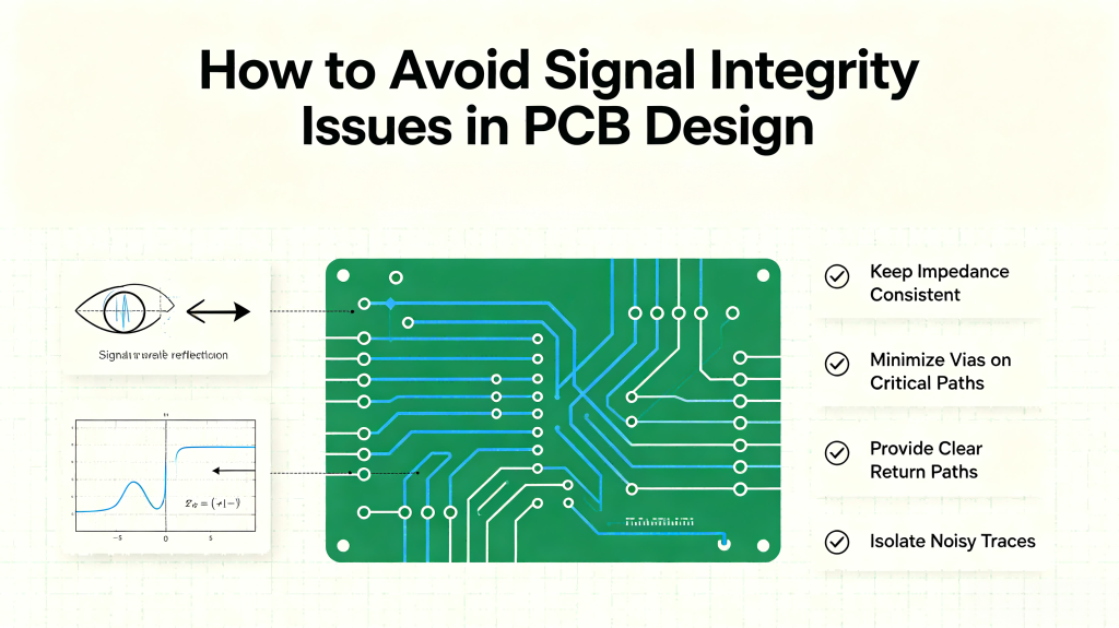
The good news is that most signal integrity problems can be reduced or avoided if the PCB is planned correctly from the beginning. This article explains the key causes of signal integrity issues in PCB design and practical ways to prevent them.
What Is Signal Integrity in PCB Design?
Signal integrity refers to the ability of an electrical signal to travel through a PCB interconnect while maintaining its intended waveform, timing, and voltage levels.
A signal with good integrity reaches the receiver with clean edges, correct amplitude, acceptable timing margin, and minimal noise. A signal with poor integrity may become distorted before it reaches its destination.
Common signal integrity problems include:
| Signal Integrity Issue | Common Cause | Possible Result |
|---|---|---|
| Reflection | Impedance mismatch | Ringing, overshoot, undershoot |
| Crosstalk | Traces routed too close together | Noise coupling, false triggering |
| Timing skew | Unequal signal lengths | Data sampling errors |
| Ground bounce | Poor grounding or fast switching current | Logic instability |
| EMI | Large loop area or discontinuous return path | EMC test failure |
| Signal loss | Long traces or high-loss materials | Eye diagram closure, reduced margin |
| Via stub resonance | Unused via barrel length | High-frequency signal distortion |
Signal integrity is not only a PCB layout issue. It is also affected by PCB materials, copper thickness, dielectric thickness, layer stackup, via structure, manufacturing tolerance, and impedance control.
That is why high-speed PCB design should always involve both the design team and the PCB manufacturer as early as possible.
Why Signal Integrity Problems Happen
Signal integrity issues usually occur when the physical behavior of the PCB interconnect is not properly controlled.
At high speeds, the signal does not simply follow the copper trace in isolation. It interacts with the surrounding dielectric material, copper geometry, reference plane, nearby traces, vias, connectors, and return current path.
Some of the most common causes include:
- Incorrect PCB stackup
- Poor impedance control
- Discontinuous reference planes
- Long or unbalanced high-speed traces
- Excessive via stubs
- Tight spacing between aggressive and victim signals
- Improper differential pair routing
- Poor decoupling capacitor placement
- Inappropriate PCB material selection
- Lack of communication with the PCB manufacturer
In other words, signal integrity is not solved by one single design rule. It requires a complete design approach.
How to Avoid Signal Integrity Issues in PCB Design
1. Start with a Proper PCB Stackup
A reliable PCB stackup is the foundation of good signal integrity.
Before routing begins, the designer should define the number of layers, signal layers, power layers, ground planes, dielectric thickness, copper weight, and target impedance values. For high-speed circuits, it is usually not a good idea to start layout first and think about stackup later.
High-speed signal layers should be placed close to a continuous reference plane, preferably a solid ground plane. This provides a short and predictable return path and helps maintain stable impedance.
For example, a simple 4-layer PCB stackup may look like this:
| Layer | Function |
|---|---|
| L1 | Signal |
| L2 | Ground |
| L3 | Power |
| L4 | Signal |
For more complex high-speed designs, 6-layer, 8-layer, 10-layer, or higher-layer-count stackups are often used to provide better routing density, cleaner reference planes, and improved EMI performance.
A good stackup helps with:
- Controlled impedance
- Lower crosstalk
- Better return current paths
- Reduced EMI
- More stable power delivery
- Better manufacturability
From a manufacturing point of view, stackup planning should also consider available laminate materials, prepreg thickness, copper thickness, board thickness tolerance, impedance tolerance, and cost.
If the PCB requires controlled impedance, the stackup should be reviewed by the PCB manufacturer before fabrication.
2. Use Controlled Impedance for High-Speed Signals
Impedance mismatch is one of the main reasons for signal reflection.
When a high-speed signal travels along a PCB trace, it expects to see a consistent characteristic impedance. If the impedance suddenly changes because of incorrect trace width, poor layer transition, via discontinuity, connector mismatch, or inconsistent dielectric thickness, part of the signal energy reflects back toward the source.
These reflections can create ringing, overshoot, undershoot, and timing errors.
Common controlled impedance values include:
| Signal Type | Typical Impedance |
|---|---|
| Single-ended signal | 50Ω |
| USB differential pair | 90Ω differential |
| Ethernet differential pair | 100Ω differential |
| LVDS differential pair | 100Ω differential |
| PCIe differential pair | 85Ω differential |
| HDMI differential pair | 100Ω differential |
The actual impedance depends on several PCB parameters:
- Trace width
- Trace spacing
- Copper thickness
- Dielectric thickness
- Dielectric constant, or Dk
- Solder mask thickness
- Trace type: microstrip, stripline, or coplanar waveguide
For controlled impedance boards, designers should not simply copy trace widths from a previous project unless the stackup and material are exactly the same.
A professional PCB manufacturer can help calculate the correct trace width and spacing based on the selected stackup. For production, impedance test coupons and TDR testing are often used to verify that the finished PCB meets the required impedance tolerance.
3. Keep the Return Path Continuous
Every signal needs a return path. For high-speed signals, the return current usually flows directly under the signal trace on the nearest reference plane.
If the signal trace crosses a split plane, slot, cutout, or gap in the reference layer, the return current has to find another path. This increases loop area and can cause noise, EMI, ringing, and crosstalk.
This is one of the most common layout mistakes in high-speed PCB design.
To maintain a clean return path:
- Route high-speed signals over solid ground planes
- Avoid crossing split planes or plane gaps
- Place stitching vias near signal layer transitions
- Keep differential pairs referenced to the same plane
- Avoid unnecessary voids under critical traces
- Use ground vias near connectors and high-speed interfaces
When a signal changes layers, its return current must also change reference planes. If the reference plane changes from one ground layer to another, place a nearby ground stitching via. If the reference changes between power and ground planes, provide suitable decoupling capacitors nearby to support the return path.
Good return path design is one of the most effective ways to reduce EMI and improve signal quality.
4. Route Differential Pairs Carefully
Differential pairs are widely used in high-speed interfaces such as USB, Ethernet, HDMI, PCIe, MIPI, SATA, LVDS, and DisplayPort.
A differential pair carries two complementary signals. The receiver detects the voltage difference between them, which improves noise immunity. However, differential routing only works well when the pair is routed correctly.
Important differential pair routing practices include:
- Maintain constant spacing between the two traces
- Keep the two traces the same length
- Avoid unnecessary bends and layer changes
- Route the pair over a continuous reference plane
- Keep the pair away from noisy signals
- Avoid routing one trace over a different plane than the other
- Match intra-pair skew according to interface requirements
It is also important to control differential impedance. A 100Ω differential pair, for example, does not automatically happen just because two traces are routed side by side. The impedance depends on trace width, spacing, copper thickness, dielectric thickness, and the reference plane.
For high-speed differential pairs, avoid using excessive serpentine tuning. Length matching is important, but too many serpentine sections can introduce additional coupling and impedance discontinuities.
The goal is not only to make two traces equal in length. The goal is to maintain a clean, balanced transmission path from transmitter to receiver.
5. Reduce Crosstalk Between Signals
Crosstalk happens when energy from one signal couples into another nearby signal. It is more serious when signals have fast edge rates, long parallel routing sections, or tight spacing.
There are two main types of crosstalk:
- Near-end crosstalk
- Far-end crosstalk
In practical PCB layout, crosstalk can cause false switching, noise, jitter, and communication errors.
To reduce crosstalk:
- Increase spacing between high-speed traces
- Avoid long parallel routing
- Route critical signals on different layers orthogonally when possible
- Use solid ground reference planes
- Keep noisy signals away from sensitive analog or clock signals
- Avoid routing high-speed traces near board edges
- Use guard traces only when properly grounded with stitching vias
A common rule of thumb is the “3W rule,” where the spacing between traces is at least three times the trace width. For more sensitive high-speed designs, larger spacing may be required.
Clock lines deserve special attention. A clock is usually a strong aggressor because it switches continuously. Keep clock traces short, well-referenced, and separated from sensitive signals.
6. Minimize Via Discontinuities and Via Stubs
Vias are necessary in most PCB designs, but they introduce parasitic inductance and capacitance. At high frequencies, vias can become significant discontinuities in the signal path.
A through-hole via may also create a via stub. A via stub is the unused portion of the plated via barrel that extends beyond the signal layer. At high data rates, this stub can behave like a resonant structure and degrade signal quality.
To reduce via-related signal integrity problems:
- Minimize the number of vias on high-speed traces
- Keep signal transitions simple and symmetrical
- Use ground stitching vias near high-speed signal vias
- Consider back drilling for very high-speed signals
- Use blind or buried vias when appropriate
- Avoid unnecessary test vias on critical high-speed nets
- Keep differential pair via transitions balanced
For interfaces such as PCIe Gen4/Gen5, high-speed Ethernet, high-frequency RF, or advanced SerDes channels, via design should be evaluated carefully. Back drilling, controlled-depth drilling, HDI microvias, or optimized via pad structures may be needed.
This is another area where PCB manufacturing capability matters. The fabricator must be able to control drill tolerance, plating quality, registration, back-drill depth, and impedance performance.
7. Keep High-Speed Traces Short and Direct
Long traces increase signal loss, delay, radiation, and exposure to noise. While some interfaces require length matching, unnecessary trace length should always be avoided.
Good routing practices include:
- Place high-speed components close to each other
- Keep critical signal paths short and direct
- Avoid unnecessary meanders
- Reduce the number of layer transitions
- Keep clocks and data lines away from noisy power circuits
- Follow the routing recommendations from the chipset or interface vendor
For memory interfaces such as DDR, trace length, topology, impedance, termination, and timing relationships must be carefully managed. For serial interfaces such as USB, PCIe, or HDMI, insertion loss, return loss, skew, and differential impedance become more important.
The right layout strategy depends on the interface type. A rule that works for one interface may not be suitable for another.
8. Use Proper Termination
Termination is used to reduce reflections by matching the impedance of the driver, transmission line, and receiver.
Common termination methods include:
- Series termination
- Parallel termination
- Thevenin termination
- AC termination
- Differential termination
The correct termination method depends on the signal type, driver strength, trace length, data rate, and receiver requirements.
For example, series termination is often used near the source for point-to-point digital signals. Differential termination is commonly used at the receiver for differential interfaces. Some modern ICs include internal termination, while others require external resistors.
Incorrect termination can be as harmful as no termination. Too much termination may increase power consumption or reduce signal amplitude. Too little termination may leave reflections uncontrolled.
Always check the IC datasheet and reference design before deciding the termination scheme.
9. Place Decoupling Capacitors Correctly
Power integrity and signal integrity are closely related. A noisy power distribution network can create jitter, ground bounce, logic errors, and EMI problems.
Decoupling capacitors help provide local transient current when ICs switch. However, they only work well when placed and routed correctly.
Good decoupling practices include:
- Place capacitors close to IC power pins
- Use short and wide connections
- Connect capacitors directly to power and ground planes with vias
- Use multiple capacitor values when needed
- Avoid long thin traces between capacitor and pin
- Keep high-frequency decoupling loops as small as possible
For BGAs and high-pin-count devices, capacitor placement should be planned early. If placement is left until the end of layout, it may be difficult to achieve a low-inductance power path.
A stable power delivery network helps reduce simultaneous switching noise and improves the timing margin of high-speed signals.
10. Choose the Right PCB Material
PCB material has a direct impact on signal integrity, especially for high-frequency and high-speed applications.
Standard FR-4 may be suitable for many digital designs, but it may not be the best choice for very high data rates, long transmission paths, RF circuits, or low-loss applications.
Important material properties include:
| Material Parameter | Why It Matters |
|---|---|
| Dk | Affects impedance and propagation delay |
| Df | Affects dielectric loss |
| Glass weave | Can cause skew in high-speed differential pairs |
| Copper roughness | Increases conductor loss at high frequencies |
| Thermal performance | Affects reliability and stability |
| Thickness tolerance | Affects impedance consistency |
For high-speed designs, low-loss materials may be required. These materials can provide better insertion loss performance and more stable electrical characteristics.
However, material selection should balance performance, cost, lead time, and manufacturability. Not every design needs expensive high-frequency laminate. In many cases, the right FR-4 grade with a carefully designed stackup is sufficient.
A good PCB supplier can help recommend suitable materials based on signal speed, impedance requirements, operating environment, and budget.
11. Avoid Routing Critical Signals Near Board Edges
High-speed traces routed too close to the board edge can radiate more easily and become more vulnerable to external noise. Board edges may also introduce impedance variation because the electromagnetic field is less contained.
As a general practice:
- Keep high-speed signals away from PCB edges
- Avoid routing clocks near the board outline
- Place ground stitching vias around board edges when needed
- Keep sensitive analog traces away from noisy digital regions
- Use proper shielding or ground structures for RF areas
This is especially important for boards that must pass EMC testing.
12. Separate Noisy and Sensitive Circuits
Mixed-signal PCB designs often include digital circuits, analog circuits, power converters, RF modules, sensors, and communication interfaces on the same board. Without careful partitioning, noise from one section can easily interfere with another.
Good placement strategy includes:
- Keep switching power supplies away from sensitive analog circuits
- Separate high-speed digital routing from low-level analog signals
- Keep crystal oscillators close to their IC pins
- Avoid routing high-current loops near signal traces
- Use solid ground planes instead of unnecessary ground splits
- Control the return current path for each functional block
Component placement often determines whether the routing will be clean or problematic. A poor placement cannot always be fixed by clever routing.
Before layout, divide the PCB into functional zones and identify critical signal paths.
13. Control Skew and Timing
In high-speed PCB design, signals often need to arrive at the receiver within a specific timing window. If related signals have different propagation delays, timing errors can occur.
Skew is especially important in:
- Differential pairs
- DDR memory buses
- Parallel data buses
- Clock and data interfaces
- High-speed connectors
To control skew:
- Match lengths where required
- Keep differential pair members close together
- Use the same layer and reference plane when possible
- Avoid unnecessary vias on one trace only
- Follow the timing rules from the device manufacturer
- Consider propagation delay differences caused by material and layer structure
Length matching should be done carefully. Excessive tuning can create unwanted coupling or impedance variations. Clean routing is usually better than visually perfect but electrically poor serpentine patterns.
14. Simulate and Review Critical Nets
For complex high-speed designs, design rules alone may not be enough. Simulation can help identify signal integrity risks before the PCB is built.
Useful analysis methods include:
- Impedance simulation
- Reflection analysis
- Crosstalk analysis
- Eye diagram simulation
- S-parameter analysis
- Power integrity analysis
- EMI risk review
Not every PCB requires full simulation. But for high-speed interfaces, dense BGAs, long channels, or strict compliance requirements, simulation can save significant time and cost.
At a minimum, critical nets should be reviewed before fabrication. This includes checking stackup, impedance, trace spacing, via transitions, return paths, length matching, and termination.
A pre-production engineering review from the PCB manufacturer can also help identify manufacturability risks that may affect signal integrity.
15. Work with Your PCB Manufacturer Early
Many signal integrity problems are related to the gap between design intent and manufacturing reality.
For example, the designer may specify a 100Ω differential pair, but the final impedance depends on the actual laminate, copper thickness, etching process, dielectric thickness, and manufacturing tolerance. If these are not aligned before production, the fabricated board may not perform as expected.
A capable PCB manufacturer can support:
- Stackup design
- Controlled impedance calculation
- Material selection
- DFM review
- Impedance coupon design
- TDR impedance testing
- HDI and microvia manufacturing
- Back drilling
- High-speed PCB fabrication
- Multilayer PCB manufacturing
- Process tolerance optimization
For high-speed PCB projects, it is better to involve the manufacturer before the layout is finalized. This helps avoid redesign, reduce prototype risk, and improve production yield.
Common Signal Integrity Mistakes to Avoid
Here are some common mistakes that often lead to signal integrity problems:
- Routing high-speed traces without a solid reference plane
- Crossing split planes with critical signals
- Using uncontrolled trace width for impedance-sensitive nets
- Placing differential pair traces too far apart
- Adding too many vias to high-speed channels
- Ignoring via stubs in multi-gigabit designs
- Routing clock lines near sensitive signals
- Placing decoupling capacitors too far from IC power pins
- Choosing PCB materials only based on cost
- Sending a controlled impedance design to fabrication without stackup confirmation
Avoiding these mistakes can greatly improve the chance of first-pass success.
PCB Manufacturing Factors That Affect Signal Integrity
Even if the layout is well designed, PCB manufacturing quality still plays an important role in signal performance.
Key manufacturing factors include:
Copper Thickness
Copper thickness affects trace impedance and conductor loss. If the actual copper thickness differs from the design assumption, impedance may shift.
Etching Tolerance
Trace width changes during etching. For fine lines and controlled impedance traces, etching compensation is critical.
Dielectric Thickness
The distance between signal trace and reference plane has a major impact on impedance. Stable dielectric thickness helps maintain predictable impedance.
Laminate Dk and Df
The dielectric constant affects impedance and signal propagation speed. The dissipation factor affects signal loss, especially at high frequencies.
Layer Registration
For multilayer boards, layer-to-layer registration affects via alignment, differential pair consistency, and overall reliability.
Via Quality
Drilling, plating, aspect ratio, and via filling quality are important for high-speed and high-reliability PCBs.
Impedance Testing
For controlled impedance PCB manufacturing, TDR testing provides verification that the finished board meets the required impedance range.
This is why choosing the right PCB manufacturer is not just a purchasing decision. It is also a signal integrity decision.
Practical Checklist for Better Signal Integrity
Before sending your PCB design to fabrication, review the following checklist:
- Is the PCB stackup finalized and approved?
- Are all high-speed signals routed over continuous reference planes?
- Are controlled impedance traces calculated based on the actual stackup?
- Are differential pairs routed with consistent spacing and length control?
- Are high-speed signals kept away from noisy circuits?
- Are clock traces short and well isolated?
- Are return paths continuous through layer transitions?
- Are stitching vias placed near high-speed vias?
- Are via stubs minimized or removed where necessary?
- Are decoupling capacitors placed close to power pins?
- Is the selected PCB material suitable for the signal speed?
- Has the PCB manufacturer reviewed the stackup and impedance requirements?
- Are impedance coupons and testing required?
- Has a DFM review been completed?
A simple checklist like this can prevent many costly problems before prototype production.
FAQ: Signal Integrity in PCB Design
What causes signal integrity issues in PCB design?
Signal integrity issues are commonly caused by impedance mismatch, poor PCB stackup, discontinuous return paths, excessive crosstalk, long traces, via stubs, poor termination, inadequate decoupling, and unsuitable PCB materials.
How do you improve signal integrity in a PCB?
You can improve signal integrity by using a proper stackup, maintaining controlled impedance, routing over solid reference planes, minimizing vias, reducing crosstalk, matching differential pairs, using proper termination, and selecting suitable PCB materials.
Why is controlled impedance important in PCB design?
Controlled impedance helps prevent signal reflections. For high-speed signals, the PCB trace behaves like a transmission line. If the impedance is not controlled, the signal may reflect, causing ringing, overshoot, undershoot, and data errors.
How does PCB stackup affect signal integrity?
The PCB stackup determines the relationship between signal traces and reference planes. It affects impedance, return path, crosstalk, EMI, and power integrity. A poor stackup can create serious signal quality problems even if the routing looks correct.
How can PCB manufacturers help prevent signal integrity problems?
A PCB manufacturer can help with stackup design, impedance calculation, material selection, DFM review, impedance coupons, TDR testing, back drilling, HDI fabrication, and process control. Early manufacturer involvement helps ensure that the fabricated PCB matches the electrical design intent.
Conclusion
Signal integrity problems in PCB design are often caused by small physical details that become critical at high speed. Trace geometry, stackup, reference planes, vias, materials, return paths, and manufacturing tolerances all influence how a signal behaves on the finished board.
To avoid signal integrity issues, designers should plan the PCB stackup early, use controlled impedance routing, maintain continuous return paths, reduce crosstalk, minimize via discontinuities, select suitable materials, and work closely with the PCB manufacturer before production.
For high-speed PCB projects, successful signal integrity is not only about good layout. It is also about matching the design with the right materials, stackup, fabrication process, and quality control.
If your project requires controlled impedance PCB, high-speed PCB fabrication, multilayer PCB manufacturing, HDI PCB, back drilling, or material selection support, working with an experienced PCB manufacturer can help reduce design risk and improve first-pass success.



0 Comments