




Introduction
The wearable electronics market has grown rapidly over the past decade, driven by consumer demand for smartwatches, fitness trackers, wireless earbuds, continuous health monitors, and augmented reality headsets. These products share a common set of engineering challenges that are fundamentally different from those found in desktop computers, industrial control systems, or even smartphones: they must be lightweight enough to wear comfortably for extended periods, thin enough to fit inside ergonomic enclosures that conform to the human body, mechanically durable enough to survive years of daily movement and environmental exposure, and electrically dense enough to integrate sensors, radios, power management, and processing in a shrinking footprint.
Traditional rigid PCBs, built on FR-4 glass-epoxy laminates, have served the electronics industry well for decades. However, they are fundamentally constrained by their flat, inflexible geometry and relatively high mass per unit area. As wearable product dimensions continue to shrink and the number of integrated functions continues to grow, rigid PCBs increasingly become a limiting factor rather than an enabling one.
Flexible printed circuit boards (FPCs) — thin, bendable circuits built on polymer substrate materials — address these limitations in a technically meaningful way. This article examines the specific technical advantages that FPCs offer in wearable device applications, with direct comparisons to traditional rigid PCB and wire harness approaches where relevant.
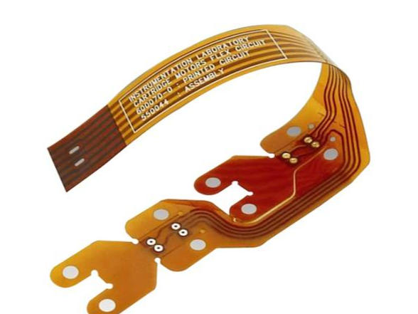
1. Material Foundation: Why Polyimide Changes the Equation
The performance characteristics of FPCs begin at the material level. The most common substrate used in high-performance FPCs is polyimide (PI), commercially known by the DuPont trade name Kapton. Polyimide offers a combination of properties that no other readily available substrate material matches for demanding flexible circuit applications:
- Thermal stability: Polyimide retains its mechanical and electrical properties across a temperature range of approximately −269°C to +400°C. This makes it compatible with standard reflow soldering processes (peak temperatures around 260°C) without dimensional distortion — a critical requirement for fine-pitch SMD component assembly on flexible substrates.
- Dielectric properties: Polyimide has a dielectric constant (Dk) of approximately 3.4 and a dissipation factor (Df) of around 0.002 at 1 GHz, suitable for moderate-frequency signal routing in wearable RF applications such as Bluetooth and BLE.
- Mechanical strength and flex endurance: Polyimide film can withstand tens of millions of flex cycles when used in dynamic bending applications, far exceeding the performance of FR-4, which will crack at the copper traces after a relatively small number of bending events.
- Thin profile: Standard polyimide base film thicknesses used in FPCs range from 12.5 μm to 125 μm, enabling total circuit thicknesses (including copper and coverlay) well below 0.2 mm — a dimension simply not achievable with FR-4 laminates.
A lower-cost alternative substrate is PET (polyethylene terephthalate), used where cost reduction is prioritized and temperature exposure is limited to below approximately 105°C. PET-based FPCs are common in disposable or low-cycle wearable patches but are not suitable for reflow assembly or high-flex-cycle dynamic applications. For most wearable devices with soldered components and long service life requirements, polyimide remains the substrate of choice.
| Property | Polyimide (PI) | PET | FR-4 |
|---|---|---|---|
| Max operating temperature | Up to +400°C | ~105°C | 130–170°C (Tg) |
| Dielectric constant (Dk @ 1 GHz) | ~3.4 | ~3.2 | ~4.5 |
| Minimum practical thickness | 12.5 μm (film only) | 25 μm (film only) | ~0.4 mm (finished board) |
| Reflow solder compatible | Yes | No | Yes |
| Dynamic flex cycles | 10 000 000+ | Limited | Not applicable |
| Relative cost | Medium–High | Low | Low |
2. Mechanical Flexibility: Static vs. Dynamic Bending
FPC designs fall into two broad mechanical categories, and understanding the distinction is important for wearable applications:
2.1 Static Flex
Static flex refers to circuits that are bent once or a limited number of times during assembly and installation, then remain in a fixed position during product operation. Examples include the cable connecting a smartwatch display to its main board, or the flex circuit routed around the battery inside a fitness tracker. Static flex designs tolerate tighter bend radii and are less constrained in terms of conductor layout rules.
2.2 Dynamic Flex
Dynamic flex refers to circuits that undergo repeated bending during normal product operation — for example, the hinge connector in a foldable display device, the interconnect in a hearing aid that flexes with jaw movement, or any circuit routed across a joint that moves with the human body. Dynamic flex designs require careful attention to:
- Minimum bend radius: Typically a minimum of 10× the total circuit thickness for copper conductors under repeated flexing.
- Conductor orientation: Traces should run perpendicular to the bend axis to minimize strain on individual conductors.
- Stress relief features: Avoiding sharp corners, using teardrop pad entries, and providing strain relief at the transition between flex and rigid regions.
- Copper type: Rolled annealed (RA) copper must be used instead of electrodeposited (ED) copper for dynamic flex applications.
RA copper is produced by mechanically rolling copper ingots to the desired thickness. Its grain structure is elongated and aligned in the rolling direction, giving it significantly better fatigue resistance than ED copper, which has a columnar grain structure more prone to crack initiation under cyclic stress. For dynamic flex applications in wearables, specifying RA copper is not a preference — it is a fundamental design requirement that directly determines product lifespan.
| Parameter | RA Copper | ED Copper |
|---|---|---|
| Grain structure | Elongated, aligned | Columnar, random |
| Flex cycle endurance | Excellent (millions of cycles) | Poor for dynamic flex |
| Surface smoothness | Smoother | Rougher |
| Cost | Higher | Lower |
| Typical application | Dynamic flex, high-reliability FPC | Static flex, rigid PCB |
3. Conductor Density and Layer Stack-Up
A key technical advantage of FPCs in wearable applications is the ability to achieve high interconnect density within a very thin cross-section. Multi-layer FPCs — available in configurations from single-layer up to 8 or more layers — allow designers to separate power, ground, and signal routing into distinct layers while maintaining a total thickness well below 0.5 mm.
A typical 4-layer FPC stack-up for a wearable application might consist of:
- 25 μm polyimide coverlay (top)
- 18 μm RA copper — signal layer 1
- 12.5 μm polyimide core
- 18 μm RA copper — ground plane
- 25 μm adhesiveless bond ply
- 18 μm RA copper — power layer
- 12.5 μm polyimide core
- 18 μm RA copper — signal layer 2
- 25 μm polyimide coverlay (bottom)
Total approximate thickness: ~0.17 mm — compared to a standard 4-layer FR-4 board at 1.0–1.6 mm.
Adhesiveless FPC constructions — where copper is deposited directly onto polyimide using sputtering or casting processes — offer further thickness reduction and improved thermal performance at higher cost. High-end FPCs can achieve trace widths and spaces of 50 μm or below on fine-line processes, supporting the high pin-count, fine-pitch interconnects demanded by the latest wearable SoCs and sensor arrays.
3. Conductor Technology: RA Copper vs. ED Copper
The choice of copper foil type is one of the most consequential material decisions in FPC design, yet it is often overlooked by engineers transitioning from rigid PCB backgrounds.
3.1 Electrodeposited (ED) Copper
ED copper is produced by electroplating copper onto a rotating drum cathode, then peeling off the resulting foil. The grain structure of ED copper is columnar — grains grow perpendicular to the foil surface. This columnar structure provides good tensile strength and is well suited to rigid PCB applications where the board does not flex. However, under cyclic bending stress, the grain boundaries between columnar grains act as crack initiation sites, causing ED copper to fail relatively quickly in dynamic flex applications.
3.2 Rolled Annealed (RA) Copper
RA copper is produced by mechanically rolling copper ingots to the desired thickness, then annealing (heat-treating) the foil to relieve internal stresses and recrystallize the grain structure. The resulting grains are elongated and aligned parallel to the rolling direction. When an RA copper trace is oriented with the rolling direction perpendicular to the bend axis, the elongated grains deform plastically under bending stress rather than fracturing along grain boundaries. This gives RA copper flex fatigue life that can be an order of magnitude or more greater than ED copper of the same thickness under equivalent dynamic flex conditions.
| Property | ED Copper | RA Copper |
|---|---|---|
| Grain structure | Columnar (perpendicular to surface) | Elongated (parallel to rolling direction) |
| Tensile strength | Higher | Lower (but sufficient for FPC use) |
| Flex fatigue resistance | Poor to moderate | Excellent |
| Surface roughness | Higher (matte side) | Lower (smoother) |
| High-frequency signal loss | Higher (due to roughness) | Lower |
| Cost | Lower | Higher (~20–40% premium) |
| Recommended application | Static flex, rigid PCB | Dynamic flex, RF signal layers |
An additional benefit of RA copper that is relevant to wearable RF designs: its smoother surface reduces the skin-effect conductor losses that become significant at Bluetooth (2.4 GHz) and UWB (6.5–8 GHz) frequencies. For antenna feed lines and RF interconnects within a wearable FPC, specifying RA copper provides both electrical and mechanical advantages over ED copper.
4. Layer Stack-Up and Density: Achieving HDI in Minimal Thickness
A key technical advantage of FPCs in wearable applications is the ability to achieve high interconnect density within a very thin cross-section. Multi-layer FPCs allow designers to separate power, ground, and signal routing into distinct layers while maintaining a total finished thickness well below 0.5 mm.
4.1 Typical Multi-Layer FPC Stack-Up
A representative 4-layer FPC stack-up for a wearable application might be constructed as follows:
- 25 μm polyimide coverlay (top protection, replacing solder mask)
- 18 μm RA copper — Signal Layer 1
- 12.5 μm polyimide base film
- 25 μm adhesiveless bond ply
- 18 μm RA copper — Ground Plane
- 12.5 μm polyimide core
- 18 μm RA copper — Power Plane
- 25 μm adhesiveless bond ply
- 18 μm RA copper — Signal Layer 4
- 25 μm polyimide coverlay (bottom protection)
Total approximate thickness: ~0.19 mm, compared to a standard 4-layer FR-4 board at 1.0–1.6 mm.
4.2 Adhesive vs. Adhesiveless Construction
Traditional FPC constructions use acrylic or epoxy adhesives to bond copper foil to the polyimide substrate. Adhesive-based constructions are lower in cost but add thickness (typically 25 μm per adhesive layer) and reduce the maximum operating temperature of the assembly to that of the adhesive (typically 105–150°C), which can be lower than the polyimide itself.
Adhesiveless constructions, in which copper is deposited directly onto polyimide by sputtering (followed by electroplating) or by casting liquid polyimide onto copper foil, eliminate the adhesive layers. The benefits for wearable applications include:
- Further reduction in total circuit thickness
- Higher thermal performance (rated by the polyimide alone)
- Better dimensional stability, critical for fine-pitch component assembly
- Improved via reliability due to better copper-to-polyimide adhesion
The trade-off is cost: adhesiveless FPCs carry a significant price premium over adhesive-based constructions, which must be weighed against the performance requirements of the specific wearable application.
4.3 Fine-Line Capability
Standard rigid PCB manufacturing processes reliably achieve trace width/space of 75 μm/75 μm (3 mil/3 mil) on outer layers. Advanced FPC manufacturers on fine-line processes can achieve 50 μm/50 μm (2 mil/2 mil) or below, enabling routing of high pin-count fine-pitch BGA and CSP devices on flexible substrates. This is increasingly important as wearable SoCs (such as those used in smartwatches) adopt 0.4 mm and 0.35 mm pitch BGA packages to minimize die size and component footprint.
5. Replacing Wire Harnesses: Reliability and Assembly Efficiency
In traditional wearable and portable device assemblies, different circuit subsystems are often connected using wire harnesses, ZIF ribbon cables, or board-to-board (B2B) connectors. While this approach is familiar and tooled for mass production, it carries significant disadvantages in wearable contexts:
- Connector contact resistance: Each B2B or ZIF connector interface introduces contact resistance (typically 20–100 mΩ per contact) that can degrade signal integrity, increase voltage drop on power rails, and add impedance discontinuities in high-speed data paths.
- Mechanical failure modes: Connector bodies can crack under drop impact; contact surfaces can oxidize or corrode when exposed to sweat and humidity; ZIF actuators can fatigue after repeated insertion/removal cycles during repair and rework.
- Assembly complexity and cost: Wire harness assembly is largely manual and difficult to automate. Each harness represents additional bill-of-materials (BOM) cost, assembly labor, and a source of variation in production quality.
- Space penalty: B2B connectors have a minimum stacking height (typically 0.4–0.8 mm for low-profile options) plus the footprint of the mating headers on both boards, consuming valuable PCB real estate inside already space-constrained wearable enclosures.
A well-designed FPC integrates multiple circuit functions into a single continuous substrate, eliminating most or all internal connectors. For example, in a smartwatch design, a single multi-layer FPC can simultaneously route the display interface, touch controller signals, heart rate sensor connections, battery management lines, and antenna feed — all within a circuit that folds to fit the watch case geometry. The result is a measurable reduction in component count, assembly steps, and potential failure points.
6. Rigid-Flex Hybrid PCBs: The Best of Both Worlds
For wearable applications that require both the high component density and soldering reliability of rigid PCB regions and the routing flexibility of FPC sections, rigid-flex PCBs offer a compelling hybrid solution. A rigid-flex board integrates rigid FR-4 (or Rogers, or other laminate) zones for component placement with flex zones for three-dimensional routing, all within a single interconnected circuit structure produced in one manufacturing process.
6.1 Construction
A typical rigid-flex construction shares conductor and dielectric layers between the rigid and flex regions. The rigid sections are built up with additional prepreg and copper layers bonded on top of the shared flex core. The transition between rigid and flex zones is a designed mechanical boundary where the coverlay and stiffener materials change. Key design considerations at the rigid-flex transition include:
- Avoiding via placement within 0.5 mm of the rigid-flex boundary to prevent stress concentration at the transition edge
- Using teardrop pad entries for traces crossing the boundary to reduce stress concentration at conductor entry points
- Specifying the transition zone angle (typically 90° to the flex axis) to distribute bending stress evenly
6.2 Advantages Over Separate Rigid PCB + FPC + Connector Approach
| Criterion | Rigid PCB + FPC + Connectors | Rigid-Flex PCB |
|---|---|---|
| Number of connector interfaces | 2 per flex section (one at each end) | Zero (continuous circuit) |
| Assembly steps | Higher (connector mating required) | Lower |
| Z-height at interconnect | 0.4–0.8 mm (connector height) | Only flex circuit thickness (~0.1–0.2 mm) |
| Signal integrity | Discontinuity at each connector | Continuous impedance-controlled routing |
| Reliability under vibration/shock | Connector-dependent | High (no connector disengagement risk) |
| NRE and unit cost | Lower NRE; moderate unit cost | Higher NRE; lower unit cost at volume |
For high-volume wearable products where reliability and miniaturization are paramount, the higher NRE (non-recurring engineering) cost of rigid-flex tooling is typically justified. Products such as premium smartwatches and professional medical wearables routinely use rigid-flex constructions for their core electronics assemblies.
7. Weight and Ergonomic Impact
The density of cured FR-4 laminate is approximately 1.85 g/cm³. Polyimide film has a density of approximately 1.42 g/cm³. For a circuit of equivalent area, the reduction in substrate thickness alone (from 1.6 mm FR-4 to 0.1 mm polyimide) reduces substrate mass by approximately 95%. When the elimination of connectors, wire harnesses, and stiffener materials is also considered, the total mass saving from adopting an FPC-based internal architecture in a wearable device can be substantial — often 2–5 grams in a smartwatch-class product, which represents a meaningful fraction of the total device weight target.
Beyond raw weight, the distributed and conformable nature of FPCs allows the electronic assembly to follow the internal geometry of the enclosure more closely, shifting mass toward the device’s center of gravity and reducing the perception of unbalanced weight on the wrist or body. This ergonomic effect is difficult to quantify but is consistently reported as a design benefit by wearable mechanical engineers.
8. Application Examples and Design Patterns
8.1 Smartwatches
Modern smartwatches typically use a rigid-flex assembly as the central electronic structure. The rigid zones carry the main SoC, PMIC, memory, and RF components; the flex zones route between the display assembly, the optical heart rate sensor on the watch back, the crown switch assembly, and the battery contacts. The flex zones are pre-formed during assembly to follow the curved interior of the watch case, with bend radii controlled to fall within the static flex design rules for the specific circuit thickness.
8.2 Wireless Earbuds
The internal volume of a wireless earbud is typically 2–4 cm³, of which the battery and speaker driver occupy the majority. The remaining space for electronics requires circuit solutions with the absolute minimum footprint and thickness. FPCs in single- or double-layer constructions are used to connect the main processor PCB to the microphone array, touch sensor, proximity sensor, and charging contacts, with each flex section pre-formed to route within the specific earbud shell geometry. The elimination of even a single B2B connector in this environment can save 0.3–0.5 mm of critical vertical space.
8.3 Continuous Health Monitoring Patches
Disposable and semi-disposable ECG patches, temperature monitors, and continuous glucose monitors (CGMs) represent a distinct FPC application where the circuit itself must be biocompatible, skin-conformable, and manufacturable at very low cost. These products commonly use PET-based single-layer FPCs with screen-printed conductive silver traces rather than etched copper, enabling roll-to-roll manufacturing processes that achieve very low per-unit costs. The circuit must conform continuously to skin movement over wear periods of 7–14 days, placing specific requirements on conductor flexibility and adhesive peel strength.
8.4 AR/VR Headsets and Smart Glasses
AR and VR headsets present one of the most complex wearable interconnect challenges: multiple high-bandwidth display interfaces (MIPI DSI or DisplayPort), camera and sensor data streams, power distribution, and audio must be routed between a processing unit (often located at the rear of the headset for weight balance) and displays, cameras, and sensors distributed across the front frame. Rigid-flex assemblies with 6–8 layers in the rigid zones and 4-layer flex sections are used in leading commercial AR headsets to manage this interconnect complexity while keeping total cable and connector count to a minimum.
9. Design and Manufacturing Considerations
Realizing the performance advantages of FPCs in wearable products requires attention to several design and manufacturing factors that differ significantly from rigid PCB practice:
- Bend zone rules: No vias, components, or solder joints should be placed within the designed flex/bend zones. Component placement must be confined to rigid zones or to areas of the FPC that will not be bent during assembly or operation.
- Stiffener placement: Areas of the FPC that require component assembly or connector mating are typically reinforced with polyimide or FR-4 stiffeners bonded to the back of the circuit. Stiffener boundaries must be carefully defined to not extend into flex zones.
- Coverlay vs. solder mask: FPCs use polyimide coverlay film (laminated and heat-pressed) rather than liquid photo-imageable solder mask for conductor protection. Coverlay openings for SMD pads must be defined in the design files and are less precise than solder mask openings — minimum coverlay-to-pad clearance is typically 0.1 mm, compared to 0.05 mm or less for solder mask.
- Impedance control: Controlled-impedance FPC designs require close collaboration with the manufacturer, as the thin and variable dielectric layers in FPCs make impedance prediction more sensitive to manufacturing tolerances than on rigid boards. Reference ground plane placement and dielectric thickness specification must be explicitly communicated in the fabrication notes.
- ESD sensitivity during handling: Polyimide is a good electrical insulator and can accumulate significant static charge during handling. FPC assemblies are more susceptible to ESD damage than rigid PCBs if proper ESD-safe handling procedures are not followed throughout the manufacturing process.
Conclusion
Flexible PCBs have evolved from a niche interconnect solution into a foundational technology for wearable electronics. Their advantages over traditional rigid PCBs and wire harness approaches are not limited to the obvious mechanical flexibility: they extend to material-level properties (polyimide thermal stability, RA copper fatigue resistance), stack-up architecture (sub-0.2 mm total thickness, fine-line HDI routing), system-level reliability (elimination of connector failure modes), and manufacturing efficiency (reduced assembly steps and component count).
The choice between pure FPC, rigid-flex hybrid, and rigid PCB with flex cable connections is not a binary one — it depends on the specific combination of flex cycle requirements, component density, signal integrity demands, production volume, and cost targets for each product. However, for any wearable device that prioritizes miniaturization, reliability, and long-term wear comfort, a thorough evaluation of FPC and rigid-flex solutions early in the design process is not optional. It is one of the highest-leverage decisions available to the design team.
As wearable devices continue to add sensing modalities, increase processing performance, and push toward smaller and lighter form factors, the role of advanced flexible circuit technology will only become more central. Engineers who develop deep competency in FPC and rigid-flex design — including material selection, conductor technology, stack-up architecture, and manufacturing process constraints — will be well positioned to deliver the next generation of wearable products that meet both the technical and human requirements of body-worn electronics.



0 Comments