




Copper thickness is one of the first details engineers check when a PCB needs to carry more than just signal-level current.
In power supplies, motor controllers, battery systems, automotive electronics and industrial control boards, the copper layer is not only a conductor.
It also affects heat generation, voltage drop, routing space, manufacturing cost and long-term reliability.
A thicker copper layer can help a PCB trace carry more current because it increases the cross-sectional area of the conductor.
With lower resistance, the trace produces less heat and has a lower voltage drop under the same current.
However, thicker copper is not always the best answer. It may increase fabrication cost, limit fine-line routing and require different design rules.
This guide explains how copper thickness affects PCB current carrying capacity and what engineers should consider before choosing
1oz, 2oz, 3oz or heavy copper PCB.
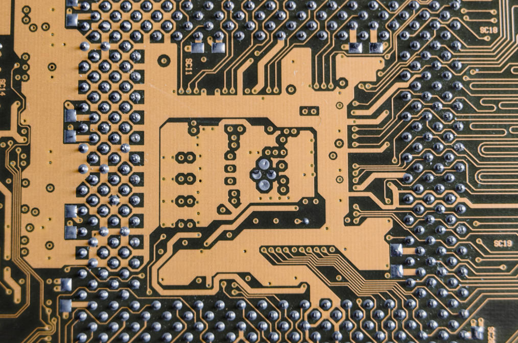
What Does PCB Copper Thickness Mean?
PCB copper thickness refers to the thickness of the copper foil on each conductive layer of a printed circuit board.
In PCB fabrication, copper thickness is commonly expressed in ounces, such as 0.5 oz, 1 oz, 2 oz, 3 oz or higher.
The term “1 oz copper” means that one ounce of copper is spread over one square foot of area.
In practical PCB manufacturing, 1 oz copper is approximately 35 μm thick.
| Copper Weight | Approximate Thickness |
|---|---|
| 0.5oz | 17.5 μm |
| 1oz | 35 μm |
| 2oz | 70 μm |
| 3oz | 105 μm |
| 4oz | 140 μm |
| 6oz | 210 μm |
For many standard PCBs, 1 oz copper is the default choice.
For higher-current designs, engineers often consider 2oz, 3oz or heavier copper depending on current level, trace width, temperature rise and available board space.
One important detail is the difference between base copper and finished copper.
Base copper refers to the copper foil before some fabrication processes, while finished copper may include additional plated copper, especially on outer layers.
When specifying copper thickness, it is better to confirm this clearly with the PCB manufacturer.
Why Copper Thickness Affects Current Carrying Capacity
A PCB trace carries current through its copper cross-section.
The larger this cross-section is, the lower the trace resistance will be.
Copper thickness directly increases that cross-sectional area.
The resistance of a PCB trace is related to the length of the trace and its cross-sectional area:
In this formula, R is trace resistance, ρ is the resistivity of copper, L is trace length, and A is the cross-sectional area of the trace.
The cross-sectional area of a trace can be simplified as:
Here, W is the trace width and T is the copper thickness.
If the trace width stays the same, increasing copper thickness increases the cross-sectional area.
This reduces resistance and allows the trace to handle more current under the same temperature-rise conditions.
This is the main reason a 2 oz copper trace can usually carry more current than a 1 oz copper trace of the same width, assuming similar board structure and cooling conditions.
Copper Thickness, Resistance and Heat
Current flowing through copper creates heat because every PCB trace has some resistance. The power loss converted into heat can be described as:
This equation is important for high-current PCB design.
If current doubles, heat generation increases by four times when resistance remains unchanged.
By increasing copper thickness, the trace resistance becomes lower.
Lower resistance helps reduce heat generation, which can improve PCB reliability and reduce the risk of overheating.
Excessive temperature rise can cause practical problems such as solder joint fatigue, laminate discoloration, delamination, component drift and reduced product lifespan.
In high-current applications, copper thickness should therefore be reviewed together with trace width, copper area, airflow, board material and component placement.
Copper Thickness vs Trace Width: Which One Matters More?
Both copper thickness and trace width affect current carrying capacity.
A wider trace gives current more copper area to flow through.
A thicker copper layer does the same by increasing the vertical dimension of the conductor.
In real PCB layout work, the better choice depends on the design constraints.
| Method | Advantage | Limitation |
|---|---|---|
| Increase trace width | Usually cost-effective and easy to fabricate | Requires more PCB space |
| Increase copper thickness | Improves current capacity when space is limited | Increases cost and affects manufacturing rules |
| Use copper pours or planes | Helps spread current and heat | Needs available layout area |
| Use multiple layers in parallel | Can distribute high current across layers | Requires proper via design and current balancing |
If the board has enough space, increasing trace width is often the more economical solution.
If the product is compact or the current is high, thicker copper may be required.
Many power PCB designs use both wider traces and thicker copper to achieve better electrical and thermal performance.
How Copper Thickness Reduces Voltage Drop
Voltage drop is another concern in high-current PCB design.
A trace may not overheat, but it can still cause performance issues if the voltage drop is too high.
Voltage drop can be calculated as:
Since thicker copper reduces trace resistance, it also helps reduce voltage drop.
This is especially useful in low-voltage, high-current circuits where even a small voltage loss can affect efficiency or system stability.
Applications where voltage drop is often critical include DC-DC converters, battery management systems, motor drive boards, LED drivers, automotive power modules and industrial power control boards.
External and Internal Layers Do Not Carry Current the Same Way
Copper thickness alone does not determine current capacity.
The layer position also matters.
External traces usually dissipate heat more easily because they are closer to air or external cooling structures.
Internal traces are surrounded by dielectric material, so heat escapes more slowly.
| Trace Location | Heat Dissipation | Design Impact |
|---|---|---|
| External layer | Better | Can usually carry more current under similar conditions |
| Internal layer | More limited | May need wider traces, thicker copper or copper planes |
For this reason, an internal 1 oz trace and an external 1 oz trace of the same width should not automatically be treated as having the same current capacity.
Internal high-current paths should be reviewed more carefully, especially in compact multilayer PCBs.
Common Copper Thickness Options by Application
There is no universal copper thickness that works for every PCB.
The right choice depends on current, temperature rise, board size, stack-up, thermal design and cost target.
| Application | Common Copper Thickness |
|---|---|
| Consumer electronics | 0.5oz to 1oz |
| Standard digital PCB | 1oz |
| Industrial control PCB | 1oz to 2oz |
| Power supply PCB | 2oz to 3oz |
| Automotive electronics | 2oz to 4oz |
| Battery management system PCB | 2oz to 4oz |
| Motor controller PCB | 3oz or higher |
| Heavy copper PCB | 4oz and above, depending on design |
These values are only general references.
Final copper thickness should be verified according to the actual current path, trace width, acceptable temperature rise and PCB fabrication capability.
When Thicker Copper Helps
Thicker copper is useful when the design needs more conductor area but cannot simply make traces wider.
This often happens in compact power boards, automotive modules and high-current industrial electronics.
Thicker copper can help when:
- The PCB must carry several amps or tens of amps.
- The available board space is limited.
- Voltage drop needs to be reduced.
- Trace temperature rise is too high with standard copper.
- The product requires better long-term power reliability.
- The design uses power devices, connectors, relays, MOSFETs or motor-driving circuits.
In these cases, 2oz, 3oz or heavy copper PCB may be a better choice than standard 1oz copper.
When Thicker Copper May Not Be the Best Choice
Thicker copper improves current carrying capacity, but it also brings trade-offs.
Specifying heavier copper without checking the full design may increase cost without solving the real problem.
Thicker copper may not be necessary when:
- The current is low and 1oz copper already meets the requirement.
- There is enough space to increase trace width.
- The PCB uses very fine traces and tight spacing.
- The design is mostly signal routing rather than power routing.
- The project is highly cost-sensitive.
- The thermal issue comes mainly from components rather than trace resistance.
In many cases, layout optimization, wider traces, copper pours, shorter current paths or better thermal vias can be more cost-effective than increasing copper thickness.
Manufacturing Impact of Thicker Copper PCBs
From a PCB fabrication point of view, thicker copper changes more than just material cost.
It affects etching, plating, solder mask, lamination and design rules.
1. Fine-Line Etching Becomes More Difficult
As copper becomes thicker, it is more difficult to maintain very fine trace width and spacing during etching.
A PCB with 3oz copper usually cannot follow the same fine-line design rules as a standard 1oz board.
2. Minimum Spacing May Need to Increase
Thick copper requires more conservative spacing to reduce the risk of etching defects and solder mask issues.
Engineers should check the manufacturer’s design rules before layout.
3. Multilayer Lamination Becomes More Challenging
In multilayer PCBs, thick copper creates greater height differences between copper and non-copper areas.
If copper distribution is uneven, resin flow during lamination can become more difficult.
4. Solder Mask Coverage Requires Attention
Thick copper edges can affect solder mask coverage and surface flatness.
This is especially important around fine-pitch components, high-current pads and dense power areas.
5. Cost and Lead Time Usually Increase
Thicker copper requires more material and stricter process control.
Heavy copper PCB manufacturing may also need longer production time and more careful inspection.
Design Tips for High-Current PCB Traces
Choosing the right copper thickness is only one part of high-current PCB design.
The layout must also provide a low-resistance and thermally balanced current path.
Use Wider Traces Where Possible
Wider traces are often the simplest way to reduce resistance and temperature rise.
If there is enough board space, increasing trace width is usually more economical than moving to heavier copper.
Use Copper Pours and Power Planes
Copper pours and planes help distribute current and spread heat.
They are especially useful for power input, ground return, MOSFET drain/source paths and high-current connector areas.
Keep High-Current Paths Short
Trace resistance increases with length.
Keeping high-current paths short and direct reduces both voltage drop and heat generation.
Avoid Narrow Bottlenecks
A high-current path is only as good as its narrowest section.
Neck-down areas near pads, connectors, fuses or components can become local hot spots.
Use Multiple Vias for Layer Transitions
If current needs to move between layers, use multiple vias in parallel.
A single via may create excessive resistance, heat and reliability risk in a high-current path.
Review Thermal Relief Connections
Thermal relief spokes are helpful for soldering, but they can restrict current flow and heat transfer.
For high-current pads, the connection style should be selected carefully.
Confirm DFM Rules Before Production
For 2 oz, 3 oz or heavy copper designs, always confirm minimum trace width, spacing, finished copper thickness, solder mask capability and stack-up with the PCB manufacturer before releasing files.
1oz vs 2oz vs 3oz Copper: Quick Comparison
| Copper Thickness | Typical Use | Main Benefit | Main Limitation |
|---|---|---|---|
| 1oz | Standard signal and low-power PCBs | Low cost and easy fabrication | Limited current capacity for power paths |
| 2oz | Medium-current power boards | Lower resistance and better current capacity | Higher cost and wider spacing may be needed |
| 3oz | High-current power electronics | Better current handling in limited space | More difficult etching and higher fabrication cost |
| 4oz and above | Heavy copper PCB applications | Suitable for very high-current designs | Specialized manufacturing capability required |
This comparison can help with early design planning, but it should not replace real current capacity calculations or manufacturer review.
Common Mistakes When Selecting PCB Copper Thickness
Choosing 1oz Copper by Default
Many designs start with 1oz copper because it is common and economical.
That works for many signal boards, but it may not be suitable for power circuits without current and temperature checks.
Assuming Thicker Copper Solves Every Thermal Problem
Thicker copper reduces trace resistance, but total board temperature also depends on component heat, airflow, copper area, board material and enclosure design.
Ignoring Internal Layer Heat Dissipation
Internal traces usually dissipate heat less effectively than external traces.
High-current internal routing should be designed more conservatively.
Using Thick Copper with Very Tight Spacing
Thick copper and fine-line routing are not always compatible.
If your board has both high-current and fine-pitch areas, discuss design rules with your PCB supplier early.
Not Specifying Finished Copper Thickness Clearly
Confusion between base copper and finished copper can lead to wrong assumptions in current capacity calculations.
The fabrication drawing should clearly state the copper requirement.
Questions to Ask Your PCB Manufacturer
Before finalizing a high-current PCB design, it is useful to confirm the following points with your manufacturer:
- What copper thickness options are available?
- Is the specified copper thickness base copper or finished copper?
- What minimum trace width and spacing are recommended for 2oz or 3oz copper?
- Can the factory support multilayer heavy copper PCB?
- Will thicker copper affect lead time or cost significantly?
- Are there any solder mask limitations for thick copper areas?
- Can the engineering team review the current path before production?
- Is copper balancing needed for the selected stack-up?
These questions can help avoid redesign, quotation changes and fabrication delays.
Conclusion
Copper thickness has a direct impact on PCB current carrying capacity.
Thicker copper increases the trace cross-sectional area, reduces resistance, lowers voltage drop and helps control temperature rise.
This makes it important for power supplies, battery systems, motor controllers, automotive electronics and other high-current PCB applications.
At the same time, thicker copper increases manufacturing complexity and cost.
It may also require larger spacing, different etching rules and more careful stack-up design.
The best choice is not always the thickest copper, but the right balance between current requirement, trace width, temperature rise, voltage drop, board space and manufacturability.
If your PCB needs to carry high current, confirm copper thickness and design rules with your PCB manufacturer before production.
Early review can reduce thermal risk, improve reliability and help control manufacturing cost.
Need Help With High-Current PCB Manufacturing?
If you are designing a high-current PCB, heavy copper PCB or power electronics board, our engineering team can help review your stack-up, copper thickness, trace width and manufacturability before production.
Send us your Gerber files, PCB stack-up and current requirements to get a manufacturing review and quotation.
FAQ: PCB Copper Thickness and Current Carrying Capacity
Does thicker copper increase PCB current carrying capacity?
Yes. Thicker copper increases the cross-sectional area of a PCB trace, which reduces resistance and allows the trace to carry more current with lower temperature rise under similar conditions.
Is 2oz copper better than 1oz copper?
2oz copper can carry more current than 1oz copper at the same trace width, but it is more expensive and may require larger spacing.
It is useful for power circuits, but not always necessary for standard signal boards.
What copper thickness should be used for high-current PCB?
Many high-current PCBs use 2oz, 3oz or heavier copper.
The final choice depends on current, trace width, temperature rise, voltage drop, layer location and manufacturing capability.
Does copper thickness affect voltage drop?
Yes. Thicker copper reduces trace resistance, and lower resistance reduces voltage drop according to:
Can thicker copper replace wider traces?
Sometimes it can help, especially when board space is limited.
However, if enough layout space is available, wider traces are often more cost-effective than simply increasing copper thickness.
Are internal traces able to carry the same current as external traces?
Not always. External traces usually dissipate heat better.
Internal traces are surrounded by dielectric material and may need wider traces, thicker copper or additional copper planes.
Does thicker copper increase PCB manufacturing cost?
Yes. Thicker copper increases material cost and can make etching, lamination, solder mask coating and inspection more demanding.
What is heavy copper PCB?
Heavy copper PCB generally refers to a PCB with copper thickness of 3oz or above, although definitions may vary by manufacturer.
It is commonly used in high-current and power electronics applications.
Conclusion
Copper thickness plays a major role in PCB current carrying capacity, trace resistance, voltage drop, and thermal performance. While thicker copper can help a PCB handle higher current and improve reliability, it should not be considered alone. Trace width, trace length, layer location, temperature rise, copper weight, and manufacturing limitations all need to be evaluated together during the design stage.
For high-current PCB applications, choosing the right copper thickness early can reduce design risks, improve power delivery, and prevent overheating issues. By working closely with an experienced PCB manufacturer, engineers can balance electrical performance, manufacturability, and cost to build more reliable circuit boards.



0 Comments