




Every PCB engineer knows the feeling: the design is finished in your head, but getting it out of your head and into Altium Designer takes hours of repetitive clicking, re-routing, and library hunting.
The good news is that most of that time is recoverable. Altium Designer ships with a deep set of automation, reuse, and interaction features that many engineers never fully adopt—often because they learned the software once and never revisited their workflow.
This guide covers 15 practical, technically verified tips to speed up your PCB design, organized in the order you actually work: setup, schematic capture, layout and routing, library management, and output. Each tip includes the exact menu path so you can find it in your version, plus the shortcuts worth committing to muscle memory.
Note on shortcuts: Altium Designer lets you fully remap keyboard shortcuts, and some defaults have shifted between releases. The menu paths below are stable references. Verify or customize shortcuts under Preferences » System » Shortcut Keys (or right-click any toolbar » Customize).
Why Design Efficiency Matters in Altium
PCB design time isn’t just labor cost—it directly affects how many design iterations you can afford before a deadline. Faster iteration means more DRC passes, more signal integrity checks, and fewer respins.
The biggest time sinks in a typical Altium workflow are almost always:
- Repetitive placement and routing of similar circuit blocks
- Manual routing of buses and connectors that could be semi-automated
- Searching for or recreating components and footprints
- Manually generating outputs (Gerbers, BOM, assembly drawings) every revision
The tips below target each of these directly.
Setup & Workspace Tips
1. Customize Your Keyboard Shortcuts
Before optimizing your workflow, optimize your input. Altium lets you remap every command.
- Go to Preferences » System » Shortcut Keys to view and edit the full list, or
- Hold Ctrl and left-click any menu item or toolbar button to open the shortcut editor for that specific command.
Assign single-key shortcuts to the commands you use dozens of times a day—place track, place via, toggle layers, run DRC. The Ctrl+click method is the fastest way to bind a shortcut to a command you just used.
2. Set Up Reusable Design Templates
Recreating title blocks, sheet borders, layer stacks, and design rules on every project is wasted effort.
- For schematics: create a template sheet and apply it across documents via Tools » Legacy Tools » Set Template Filename (path varies by version; also configurable in Preferences » Schematic).
- For the board: save a
.PcbDocwith your standard layer stack, design rules, and board outline as a starting point. - For company-wide standardization, store templates in a shared location or a managed content server so the whole team pulls from the same source.
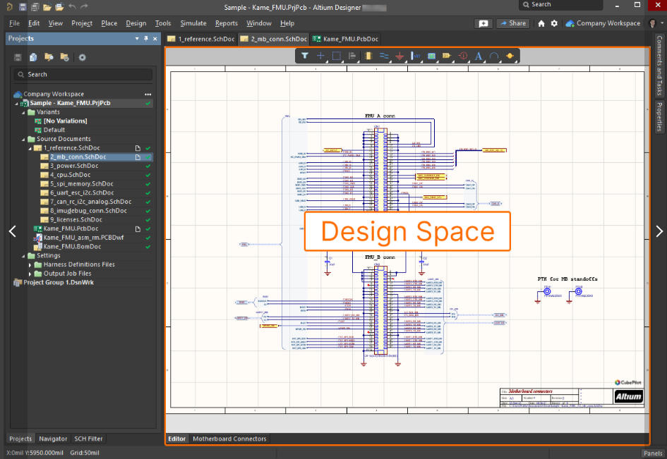
3. Organize Your Panels and Workspace Layout
Altium’s panels (Projects, Properties, PCB, Navigator) can be docked, floated, or auto-hidden. A cluttered or default layout costs you clicks every session.
- Access panels via the Panels button in the bottom-right corner.
- Dock the panels you use constantly (Properties, PCB) and auto-hide the rest.
- On a dual-monitor setup, float the schematic on one screen and the PCB on the other to eliminate document switching.
Schematic Capture Tips
4. Use Snippets to Reuse Circuit Blocks
Snippets are one of Altium’s most underused time-savers. Any block of circuitry—a power supply stage, a common connector with its passives, a microcontroller reset network—can be saved and reused.
- Select the circuitry, then right-click » Snippets » Create Snippet from selected objects.
- Reuse it later by dragging it from the Snippets panel (open via Panels » Snippets) into any schematic or PCB.
This works for both schematic and PCB objects, so you can reuse proven layout patterns too.
5. Master Multi-Channel Design for Repeated Circuits
If your design has repeated identical channels—audio inputs, LED drivers, sensor front-ends—do not copy and paste them. Use multi-channel design instead.
- Create the channel circuit once on a sub-sheet.
- On the top sheet, place a sheet symbol referencing it and set its designator using the Repeat keyword, for example:
Repeat(Channel, 1, 8)to generate eight instances. - Compile the project (Project » Compile PCB Project) to expand the channels.
The real payoff comes in layout: route and place one channel, then use Design » Rooms » Copy Room Formats to replicate that exact placement and routing across all channels. This can turn hours of repetitive layout into minutes.
6. Use Cross-Probing and Cross-Select Mode
Jumping between a component in the schematic and its footprint on the board is a constant action. Cross-select links the two.
- Enable it under Tools » Cross Select Mode (or in Preferences » System » Navigation).
- With it on, selecting an object in the schematic highlights and selects the corresponding object on the PCB, and vice versa.
For a one-off jump, use Tools » Cross Probe and click the object you want to locate in the other document.
PCB Layout & Routing Tips
This is where most design time is spent, so these tips carry the highest return.
7. Speed Up Routing with ActiveRoute
ActiveRoute routes multiple selected connections along a path you define—far faster than manual routing for buses, memory interfaces, and connector breakouts.
Workflow:
- Open the ActiveRoute panel via Panels » PCB ActiveRoute.
- Select the connections (ratsnest lines) or nets you want routed.
- Optionally guide the routing by drawing a guide path so ActiveRoute follows your intended direction.
- Click ActiveRoute in the panel.
ActiveRoute respects your design rules for clearance and width, so the output is manufacturable, not just fast. It’s best for groups of related nets—use interactive routing for critical single traces where you want full control.
8. Learn the Interactive Routing Shortcuts
Interactive routing (Route » Interactive Routing, default shortcut Ctrl+W or the toolbar) becomes dramatically faster once you know its in-command keys. While actively routing a trace:
- Shift+Space — cycle the corner/routing mode (45°, 45° with arc, 90°, 90° with arc, any angle, rounded).
- Space — toggle the corner direction (switch which end the corner is applied to).
- Tab — open Properties mid-route to change trace width, via size, or layer without stopping.
*(numpad) — add a via and switch to the next signal layer in one action.+/-(numpad) — move to the next/previous signal layer (inserts a via).- Backspace — remove the last placed track segment.
- Shift+R — cycle the conflict-resolution mode (stop at obstacle, walk around, push, hug-and-push).
- Ctrl+left-click on the target pad — attempt to auto-complete the current net.
9. Use Rooms for Modular Layout
Rooms group components so you can move, arrange, and constrain them as a unit—ideal for functional blocks or repeated channels.
- Create one via Design » Rooms » Place Rectangular Room, or assign components to a room through a design rule scope.
- Moving the room moves all its components together, which keeps related circuitry physically grouped and simplifies floor-planning.
10. Manage Polygon Pours with the Polygon Pour Manager
Manually placing and repouring copper pours one at a time is slow and error-prone.
- Open Tools » Polygon Pours » Polygon Pour Manager to view, name, reorder, repour, and shelve/unshelve every polygon on the board from a single dialog.
- Use shelve to temporarily hide pours while routing (much faster redraws), then unshelve and repour before verification.
Pour order matters for layered planes—the manager lets you set it explicitly rather than relying on placement order.
11. Route Differential Pairs Correctly and Quickly
For high-speed signals, route pairs together with matched length and spacing rather than as two independent traces.
- Define the pair with Place » Directives » Differential Pair, or name the two nets with matching
_P/_Nsuffixes and add them to a differential pair class. - Route with Route » Interactive Differential Pair Routing—Altium maintains the gap and routes both traces simultaneously.
- Set gap and width targets through a Differential Pair Routing design rule so the interactive tool enforces your impedance target.
Library & Component Management Tips
12. Centralize Your Component Libraries
Scattered .SchLib and .PcbLib files lead to duplicate parts and mismatched footprints. Consolidate into a single source of truth.
- For teams, use a managed component library on an Altium content server so symbol, footprint, and supplier data live in one linked component.
- For individual use, at minimum maintain a single integrated library (
.IntLib) or a defined library search path via Preferences » Data Management » File-based Libraries.
Centralized libraries mean every reused part already carries a verified footprint—eliminating one of the most common sources of respins.
13. Use the Manufacturer Part Search Panel
Instead of manually building common components, pull them—with real supplier and parametric data—directly into your design.
- Open Panels » Manufacturer Part Search.
- Search by part number or parameters, review lifecycle and availability data, and place the component with its symbol and footprint attached.
This also keeps your BOM aligned with real, sourceable parts from the start.
Verification & Output Tips
14. Automate Checks with Design Rules and DRC
The fastest way to catch errors is to prevent them during layout. Well-configured design rules turn the router into a real-time checker.
- Define rules under Design » Rules—clearance, width, via styles, differential pairs, plane connections, and more.
- Keep online DRC enabled so violations flag as you route.
- Run a full batch DRC before output via Tools » Design Rule Check.
Investing time in your rule set up front saves far more time than manually inspecting a finished board.
15. Use Output Job Files for One-Click Documentation
Regenerating Gerbers, NC drill files, BOM, and assembly drawings by hand on every revision is pure repetition. An Output Job file automates all of it.
- Create one via File » New » Output Job File.
- Add every output you need—Gerber, NC Drill, BOM, PDF, assembly drawings, IPC-2581 or ODB++—and link them to output containers (folder, PDF, or ZIP).
- On each revision, generate the complete release package in a single action.
Set this up once per project template and your entire manufacturing package becomes a one-click export.
Essential Altium Designer Shortcuts Cheat Sheet
Well-established defaults for interactive routing and PCB navigation. Confirm or remap under Preferences » System » Shortcut Keys.
| Action | Shortcut | Context |
|---|---|---|
| Cycle corner/routing mode | Shift+Space | While routing |
| Toggle corner direction | Space | While routing |
| Edit properties mid-command | Tab | While routing/placing |
| Add via + change layer | * (numpad) | While routing |
| Next / previous signal layer | + / - (numpad) | While routing |
| Remove last track segment | Backspace | While routing |
| Cycle conflict resolution | Shift+R | While routing |
| Auto-complete current net | Ctrl+left-click target | While routing |
| Toggle units (mil / mm) | Q | PCB editor |
| 2D / 3D view | 2 / 3 | PCB editor |
| Toggle single-layer mode | Shift+S | PCB editor |
| Rotate object 90° | Spacebar | While moving/placing |
| Flip to other side | L | While dragging a component |
| Mirror object | X / Y | While moving/placing |
| Cycle snap grid | G | PCB editor |
| Place wire (schematic) | P, W | Schematic editor |
| Place net label (schematic) | P, N | Schematic editor |
Frequently Asked Questions
How do I route faster in Altium Designer? Use ActiveRoute (Panels » PCB ActiveRoute) to route groups of related nets along a guide path, and learn the interactive routing in-command keys—Shift+Space to change corner mode, Tab to adjust width or layer mid-route, and the numpad * key to drop a via and switch layers in one step.
What are the most useful Altium keyboard shortcuts? For routing: Shift+Space (corner mode), Tab (properties), * (via + layer change), and Shift+R (conflict resolution). For navigation: Q (toggle units), 2/3 (2D/3D view), and Spacebar (rotate). All are remappable under Preferences » System » Shortcut Keys.
Can I reuse circuit designs across projects in Altium? Yes. Use Snippets (right-click » Snippets » Create Snippet) for reusable schematic or PCB blocks, and multi-channel design with the Repeat keyword for identical repeated circuits. Design » Rooms » Copy Room Formats replicates a channel’s placement and routing across all its instances.
How do I speed up generating manufacturing files? Set up an Output Job file (File » New » Output Job File) with all your Gerber, NC drill, BOM, and assembly outputs linked to output containers. You can then regenerate the full release package in one action on every revision.
Conclusion
Speeding up your PCB design in Altium isn’t about clicking faster—it’s about replacing repetition with reuse and automation. The highest-impact changes are usually multi-channel design and Copy Room Formats for repeated circuits, ActiveRoute for bus and connector routing, a centralized component library, and Output Job files for one-click releases.
Pick two or three tips from this list that match your biggest time sinks and adopt them on your next design. Once they’re in your muscle memory, layer in the rest. The compounding effect across a full project—and across a year of projects—is substantial.
Which of these will you try first? Start with the routing shortcuts if you spend most of your day in the PCB editor; start with snippets and templates if you find yourself recreating the same circuits again and again.



0 Comments