




Surface Mount Technology (SMT) assembly is at the heart of modern electronics manufacturing. From smartphones and automotive ECUs to industrial control boards and medical devices, SMT enables high-density, high-reliability circuit board production at scale.
But even in a well-controlled SMT line, defects happen.
A single process deviation—whether in solder paste printing, component placement, or reflow profiling—can result in defective joints that reduce yield, drive up rework costs, or cause failures in the field.
According to industry data, solder joint defects account for more than 70% of all PCB assembly failures. Identifying these issues early, understanding their root causes, and applying targeted solutions is essential for any manufacturer looking to stay competitive in 2026.
This guide covers the top 10 SMT assembly defects, their causes, and proven solutions you can implement today.

What Causes SMT Defects? A Quick Overview
SMT defects rarely have a single cause. They typically result from a combination of factors across five key process areas:
- Solder paste printing – paste volume, stencil design, printer settings
- Component placement – machine calibration, nozzle condition, fiducial accuracy
- Reflow soldering – temperature profile, conveyor speed, nitrogen atmosphere
- PCB and component quality – surface finish, oxidation, moisture absorption
- Design for Manufacturability (DFM) – pad geometry, copper balance, component spacing
Understanding which process stage is responsible for a defect is the first step toward fixing it permanently.
1. Solder Bridging
What Is Solder Bridging?
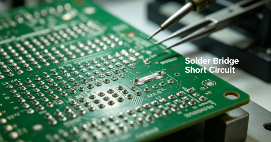
Solder bridging occurs when excess solder forms an unintended electrical connection between two adjacent pads or component leads. The result is a short circuit that can damage components, cause system malfunction, or create a fire hazard in high-current applications.
Bridging is especially common on fine-pitch ICs, QFN packages, BGAs, and densely populated 0402 or 0201 passive arrays.
Root Causes of Solder Bridging
- Excessive solder paste deposition due to oversized stencil apertures
- Stencil misalignment or poor gasket seal
- Inadequate solder paste viscosity or incorrect paste type
- Reflow profile with too-aggressive ramp rate, causing paste spread
- Flux residue promoting solder flow between adjacent pads
- Poor component placement accuracy on fine-pitch devices
Proven Solutions
- Reduce stencil aperture dimensions for fine-pitch pads — typically 80–90% of pad size
- Use a thinner stencil (e.g., 100 µm instead of 130 µm) to reduce paste volume
- Verify stencil-to-board alignment with an SPI (Solder Paste Inspection) system before every production run
- Adjust reflow soak zone to allow flux activation before full solder melt
- Calibrate placement machines regularly to maintain positioning accuracy
- Implement 100% AOI after reflow to catch bridges before board-level testing
2. Tombstoning (Manhattan Effect)
What Is Tombstoning?
Tombstoning — also called the Manhattan effect or drawbridge effect — occurs when a small chip component (resistor, capacitor, or inductor) lifts off one pad during reflow and stands vertically. The result is a completely open circuit on the lifted end.
This defect is most common with 0402, 0201, and 01005 passive components.
Root Causes of Tombstoning
- Unequal solder paste volumes on the two pads of a two-terminal component
- Unbalanced thermal mass — one pad connected to a large copper pour heats more slowly
- Poor PCB pad design with asymmetric geometry
- Component placement offset or rotation error
- Overly fast reflow ramp rate causing rapid, uneven solder wetting
- Differences in surface finish solderability between the two pads
Proven Solutions
- Ensure symmetric pad geometry and copper distribution on both sides of the component
- Use identical stencil apertures for both pads to achieve equal paste volume
- Verify component placement accuracy — offset greater than 25% of pad width increases tombstone risk
- Slow down the reflow ramp rate in the preheat zone to allow more uniform heating
- Run a thermal profile across the board to confirm temperature uniformity at component locations
- Review IPC-7351 land pattern recommendations for all passive components
3. Insufficient Solder Joints
What Is an Insufficient Solder Joint?
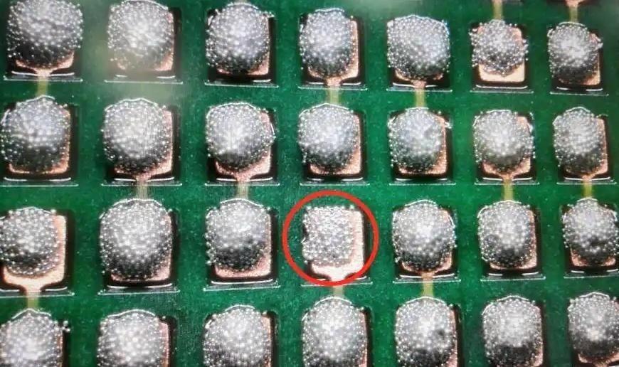
An insufficient solder joint occurs when there is not enough solder to form a complete, reliable connection. The joint may look visually acceptable but lacks the mechanical and electrical integrity required for long-term operation.
These joints are prone to cracking under thermal cycling, vibration, or mechanical stress — making them a significant reliability risk.
Root Causes
- Blocked or partially clogged stencil apertures
- Low solder paste volume due to worn stencil or incorrect printer settings
- Poor paste release from the stencil, especially for high aspect ratio apertures
- Reflow peak temperature too low to fully melt the alloy
- Oxidized PCB pads or component leads reducing wettability
- Solder paste past its shelf life or improperly stored
Proven Solutions
- Inspect and clean stencils after every production run — ultrasonic cleaning recommended for fine apertures
- Monitor paste deposits with SPI — reject boards where volume is below 75% of nominal
- Adjust squeegee pressure and speed to optimize paste release
- Verify oven peak temperature using calibrated thermocouples at multiple board locations
- Follow FIFO (First In, First Out) management for solder paste inventory
- Store PCBs in sealed packaging with desiccant to prevent pad oxidation
4. Solder Balls
What Are Solder Balls?
Solder balls are small, spherical deposits of solder scattered around component leads, pads, or across the PCB surface after reflow. They may cause intermittent shorts, reduce creepage distance, and create cosmetic quality failures — especially in aerospace, medical, and automotive electronics.
Root Causes
- Excess solder paste volume deposited during printing
- Moisture in solder paste, PCB materials, or components
- Too-rapid ramp rate during reflow, trapping flux volatiles
- Contaminated PCB surface (oils, fingerprints, residues)
- Paste smearing during stencil separation
- Incompatible flux chemistry for the reflow atmosphere
Proven Solutions
- Control paste volume with regular SPI measurement and stencil inspection
- Allow solder paste to reach room temperature before opening the container (typically 2–4 hours from refrigerator)
- Bake moisture-sensitive PCBs prior to assembly if humidity exposure is suspected
- Optimize the reflow soak zone — allow enough time for volatiles to escape before the liquidus stage
- Keep production areas clean and handle PCBs with gloves to prevent contamination
- Use nitrogen atmosphere in the reflow oven for moisture-sensitive or lead-free assemblies
5. Component Misalignment
What Is Component Misalignment?
Component misalignment occurs when an SMT component is placed off-center, incorrectly rotated, or shifted from its target position. Depending on severity, misalignment can cause open circuits, solder bridges, poor joint formation, or complete functional failure.
Root Causes
- Pick-and-place machine calibration drift
- Worn or damaged placement nozzles causing drop or rotation errors
- Incorrect package data or footprint mismatch in the machine library
- Poor fiducial mark recognition due to damaged marks or camera calibration issues
- PCB panel registration problems
- Solder paste imbalance pulling the component off-center during reflow (self-alignment failure)
Proven Solutions
- Calibrate pick-and-place machines daily using reference boards
- Inspect nozzles for wear, contamination, or blockage on a regular schedule
- Validate component library data against datasheet dimensions before first production
- Verify fiducial marks — ensure they are clean, clearly defined, and properly recognized
- Use PCB fixtures or pallets to maintain consistent panel position during placement
- Deploy post-placement AOI before reflow to catch misalignment before solder sets
6. Open Solder Joints
What Is an Open Solder Joint?
An open solder joint is an incomplete electrical connection — the component lead, pad, or solder ball fails to form a continuous conductive path. Unlike solder bridges, open joints cause circuit failures rather than shorts. They are particularly dangerous because they can be intermittent, making them difficult to detect during electrical testing.
Root Causes
- Insufficient solder paste volume
- Poor wetting due to oxidized pads or leads
- Incorrect reflow peak temperature or time above liquidus (TAL)
- PCB or package warpage preventing contact during reflow
- Head-in-pillow defects in BGA assemblies (discussed in defect #9)
- Excessive component coplanarity variation
Proven Solutions
- Monitor solder paste volume consistently with SPI
- Verify component and PCB solderability with incoming inspection
- Develop a validated reflow profile — ensure peak temperature and TAL meet solder paste manufacturer specifications
- Check PCB warpage before assembly, especially for large or thin boards
- Use X-ray inspection to detect hidden open joints in BGA, QFN, and LGA packages
- Bake components according to MSL (Moisture Sensitivity Level) requirements before assembly
7. Cold Solder Joints
What Is a Cold Solder Joint?
A cold solder joint occurs when solder does not fully melt or properly wet the pad and component lead during reflow. These joints typically appear dull, gritty, or grainy in appearance — in contrast to a healthy, bright, smooth joint. They are mechanically weak and electrically unreliable, often failing under vibration or thermal cycling.
Root Causes
- Reflow peak temperature below the solder alloy’s liquidus point
- Insufficient time above liquidus (TAL too short)
- Poor heat transfer to high-mass components or thick copper areas
- Oxidized component leads or PCB pads
- Incompatible solder paste alloy and reflow profile combination
- Oven belt speed too fast for the board’s thermal mass
Proven Solutions
- Develop a board-specific reflow profile using thermocouples at multiple locations
- Ensure correct TAL — typically 45–90seconds for most SAC305 lead-free alloys
- Add thermal relief vias for large copper pours and thermal pads
- Reduce conveyor speed or addoven zones for complex, high-mass boards
- Inspect regularly with AOI and cross-section analysis to catch cold joints early
- Use flux-core wire or no-clean flux for any manual rework to improve wetting
8. Voiding in Solder Joints
What Are Solder Voids?
Voids are gas pockets trapped inside a solder joint. While small voids (below IPC-7093 acceptance criteria) are generally acceptable, excessive voiding reduces thermal conductivity, increases electrical resistance, and weakens mechanical integrity — all critical in power devices, QFNs, thermal pads, LEDs, and automotive electronics.
Root Causes
- Flux volatiles trapped in the joint during solidification
- Moisture in PCB laminates or component packages
- Large thermal pad areas with insufficient outgassing paths
- Solid stencil apertures on full-coverage thermal pads
- Reflow profile with insufficient outgassing time
- Wrong solder paste formulation for the application
Proven Solutions
- Select low-void solder paste formulations specifically designed for thermal pad applications
- Use window-pane (cross-hatched) stencil apertures on large thermal pads — typically 4–9 openings covering 50–80% of pad area
- Optimize the reflow soak stage to allow volatiles to escape before liquidus
- Bake moisture-sensitive boards and components per IPC/JEDEC J-STD-020
- Consider vacuum reflow for demanding applications requiring void levels below 5%
- Inspect with X-ray — measure voiding percentage per IPC-7093 standards
9. BGA Head-in-Pillow (HIP) Defects
What Is a Head-in-Pillow Defect?
Head-in-pillow (HIP) is a subtle but serious BGA defect. During reflow, the BGA solder ball (the “head”) and the solder paste on the PCB pad (the “pillow”) both melt separately but fail to fully coalesce into a single joint. The result is a joint that may look connected visually or even on standard AOI, but is actually an open or near-open connection.
HIP defects are one of the most difficult SMT defects to detect without X-ray inspection.
Root Causes
- PCB or BGA package warpage causing separation during reflow
- Oxidized BGA solder balls reducing wettability
- Inadequate reflow peak temperature or TAL for large BGAs
- Uneven heating across the board causing different areas to reach liquidus at different times
- Moisture-induced package deformation (popcorning)
- Insufficient solder paste volume on BGA pads
Proven Solutions
- Mandatory X-ray inspection for all BGA packages — 2D X-ray as minimum, 3D CT X-ray for critical assemblies
- Store BGAs and PCBs in controlled humidity environments (≤10% RH with desiccant)
- Bake BGAs according to MSL rating — especially important for large, fine-pitch BGAs
- Optimize reflow profile for large BGAs — consider longer soak and higher peak temperature
- Use nitrogen atmosphere reflow to prevent ball oxidation
- Verify BGA coplanarity with incoming inspection using a 3D inspection system
10. PCB Warpage and Delamination
What Are PCB Warpage and Delamination?
PCB warpage is the bending or twisting of a board under thermal stress. Delamination is the internal separation of PCB laminate layers. Both conditions affect the reliability of solder joints, the accuracy of component placement, and the long-term structural integrity of the assembly.
Warpage is especially problematic for large boards, thin PCBs, and assemblies with multiple reflow passes.
Root Causes
- High moisture absorption in PCB laminate before assembly
- Incorrect PCB material selection for the thermal demand
- Unbalanced copper distribution across PCB layers
- Excessive reflow temperatures exceeding the laminate’s Tg (glass transition temperature)
- Multiple reflow cycles accumulating thermal stress
- Improper PCB thickness or layer stack-up design
Proven Solutions
- Select PCB laminates with appropriate Tg, CTE, and thermal stability for the process
- Store PCBs in sealed, dry packaging — bake boards at 120°C for 4–6 hours if moisture exposure is suspected
- Balance copper distribution across all PCB layers to minimize differential thermal expansion
- Use PCB carrier fixtures for thin boards (under 1.0 mm) during reflow
- Minimize unnecessary reflow cycles — plan assembly sequence to reduce total heat exposure
- Review PCB stack-up design with your fabricator before finalizing the design
How to Prevent SMT Defects: A Systematic Approach
Fixing defects after they occur is costly and reactive. Best-in-class SMT manufacturers build quality control into every stage of the process. Here is a proven framework:
Step 1: Implement SPI, AOI, and X-Ray Inspection
| Inspection Tool | Stage | What It Detects |
|---|---|---|
| SPI (Solder Paste Inspection) | Post-print | Paste volume, alignment, bridging |
| AOI (Automated Optical Inspection) | Post-reflow | Missing parts, polarity, bridging, misalignment |
| X-Ray | Post-reflow | BGA voids, HIP, hidden solder joints |
SPI is particularly valuable — catching solder paste problems before placement prevents the majority of downstream defects.
Step 2: Control Materials and Storage
- Keep solder paste refrigerated (typically 2–10°C) and track shelf life with FIFO
- Store PCBs in sealed packaging with humidity indicator cards
- Follow JEDEC MSL requirements for all moisture-sensitive components
- Document material traceability for every production batch
Step 3: Optimize the Reflow Profile
No single reflow profile works for all boards. Key variables to consider:
- Board thickness and layer count
- Component density and package types
- Solder alloy composition (SAC305, SAC405, low-temperature alloys)
- PCB surface finish (HASL, ENIG, OSP, immersion silver)
- Use of nitrogen atmosphere
Always validate profiles using real thermocouples attached to critical components — not just oven recipe settings.
Step 4: Apply Design for Manufacturability (DFM)
Many SMT defects are designed in before production ever starts. A thorough DFM review should address:
- Pad and footprint accuracy per IPC-7351
- Component-to-component spacing and keepout zones
- Balanced pad geometry for two-terminal passives
- Thermal pad and stencil aperture design
- Fiducial mark size, placement, and copper-free keepout
- BGA fanout and via-in-pad design rules
Step 5: Use Process Data and Traceability
Modern SMT factories in2026 leverage machine connectivity and real-time data collection to monitor:
- Solder paste volume trends across the stencil
- Placement accuracy distributions per nozzle and component type
- Reflow temperature profiles per board design
- First-pass yield and defect Pareto data by defect type
This data enables proactive process control — identifying drift before it becomes a defect.
FAQ
What is the most common SMT defect in PCB assembly?
Solder bridging and insufficient solder joints are consistently the most common SMT defects, particularly on fine-pitch components and densely packed boards.
How can I reduce tombstoning defects?
Tombstoning is primarily caused by unequal heating or unequal solder volumes on the two pads of a chip component. Ensure symmetric pad design, equal paste volumes, and a controlled reflow ramp rate.
Is X-ray inspection necessary for all SMT assemblies?
X-ray is essential for assemblies with BGA, QFN, LGA, or large thermal pads where solder joints are hidden from surface inspection. For standard through-hole or visible SMT joints, AOI is typically sufficient.
What does TAL mean in reflow soldering?
TAL stands for Time Above Liquidus — the duration during which solder remains in its molten state during reflow. Most lead-free SAC alloys require 45–90 seconds of TAL for complete wetting and joint formation.
How do I fix a cold solder joint?
Cold solder joints should be reflowed with additional flux or replaced using a soldering iron with appropriate flux-core solder. The root cause — usually a reflow profile issue or surface oxidation — must also be addressed.
Conclusion
SMT assembly defects are a fundamental challenge for every electronics manufacturer. Whether you are running high-volume consumer electronics or low-volume industrial systems, the same10 defects — solder bridging, tombstoning, insufficient solder, solder balls, misalignment, open joints, cold joints, voiding, BGA head-in-pillow, and PCB warpage — account for the vast majority of quality escapes.
The path to reliable, high-yield SMT production runs through process control, not rework. By addressing root causes — optimizing your paste printing, placement, and reflow stages, implementing inline inspection, and designing for manufacturability — you can dramatically reduce defect rates and improve first-pass yield.
If you are evaluating your current SMT process or planning a new production line, start with a structured audit of these 10 defect categories. The data you collect will guide you directly to the improvements that matter most.
Have questions about SMT assembly quality or process optimization? Contact our engineering team — we are happy to help you diagnose and solve your specific production challenges.



0 Comments