




What Does PCB Components Identification Actually Confirm?
PCB components identification means proving what a mounted part is to the level required by the job. That may be only its family, such as resistor or diode, or it may require the exact manufacturer part number, value, package, voltage rating, tolerance, polarity, and approved substitute.
These are different conclusions. A black three-pin SMD package may look like a transistor, but the same package can contain a transistor, diode pair, voltage regulator, voltage detector, or other IC. Shape provides a candidate; it does not provide a purchase-ready identity.
- Family identified: you can say what kind of function the part probably performs.
- Value or key specification identified: you have decoded or measured a useful parameter, such as 10 kΩ.
- Exact part identified: the manufacturer, full MPN, package, ratings, and revision evidence agree.
- Orientation identified: Pin 1, cathode, or positive/negative terminal is confirmed from package and board documentation.
For learning or preliminary repair, a probable family may be useful. For sourcing, substitution, assembly, or production release, “probably the same” is not enough. Use the evidence ladder below to decide how strong your conclusion really is.
What Evidence Should You Trust First?
Trust revision-controlled design documents and manufacturer information before appearance, search results, or a single meter reading. The strongest practical identification usually comes from several independent clues that agree.
| Evidence | What it can confirm | Typical strength | Main limitation |
| Correct-revision BOM or approved vendor list | Exact MPN, description, package, value, rating, approved alternative | Very strong | Wrong board revision or an uncontrolled BOM can still mislead |
| Assembly drawing and schematic | Location, RefDes, function, connectivity, orientation | Very strong | May use an internal part description rather than full ordering code |
| Manufacturer datasheet or marking lookup | Top mark, package, pinout, ratings, polarity, date/lot-code structure | Strong | You must already have a credible manufacturer or part candidate |
| Package, pin count, logo, top mark, nearby circuit | A shortlist of plausible parts | Medium | Short codes and packages are frequently reused |
| Unpowered multimeter or LCR measurement | Continuity, junction behavior, approximate resistance or capacitance | Supporting | Parallel circuit paths can change the reading |
| Visual similarity, web image search, code database | A search lead | Weak by itself | Look-alikes and duplicate top codes produce false matches |
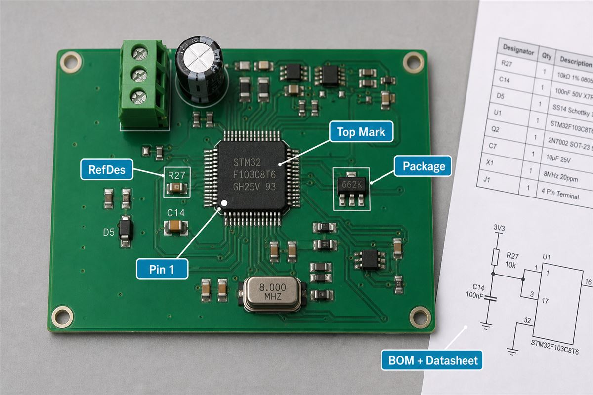
A practical sequence is: board revision → reference designator → package and pin count → body marking and logo → polarity or Pin 1 → BOM/schematic/assembly drawing → manufacturer datasheet → limited measurement. Do not stop at the first clue that seems to fit.
How Do You Record the Board Before Identifying Parts?
Record the board before cleaning, removing, or rotating anything. Component identity depends on location and board revision, and those clues can disappear during repair.
- Disconnect power. Remove external power and batteries. Do not identify unknown components by probing a live board.
- Photograph the whole board. Capture both sides, connectors, labels, and the component’s relationship to nearby parts.
- Capture close-ups. Use straight-on lighting, several angles, and one image that shows the RefDes next to the part.
- Record board identity. Write down the product, PCB number, revision, serial/lot information, and side of the board.
- Mark the location. Record the grid position or highlight the component on a copy of the board photo.
- Preserve orientation. Note the band, dot, notch, chamfer, or terminal direction before removing the component.
“R12 on revision A” and “R12 on revision C” do not have to be the same value or part. A close-up with no board context is also harder to diagnose because the surrounding circuit often tells you whether a package belongs to a power rail, signal path, oscillator, protection network, or connector interface.
How Do You Read Reference Designators Without Mistaking Them for Part Numbers?
A reference designator identifies a component position in the design. Its letters usually suggest the component family, while its number distinguishes that position from other parts of the same family. It normally does not state the value or exact part number.
For example, R23 means “the resistor at position 23” in the project documentation. It does not mean 23 Ω. The BOM entry for R23 might specify 10 kΩ, 1%, 0603, and a particular MPN.
| Common prefix | Usual component family | What it does not prove |
| R | Resistor | Resistance, tolerance, power rating, or MPN |
| C | Capacitor | Capacitance, dielectric, voltage rating, or polarity |
| L | Inductor | Inductance, current rating, or whether it is a ferrite bead |
| D or CR | Diode, LED, or rectifier | Diode type, voltage/current rating, or band meaning without context |
| Q | Transistor or related discrete semiconductor | BJT versus MOSFET, channel type, pinout, or MPN |
| U or IC | Integrated circuit or module | Function, pinout, supply voltage, or firmware |
| J, P, or CN | Connector | Mating part, pin assignment, or current rating |
| F | Fuse | Current, voltage, speed, or interrupt rating |
| TP | Test point | Expected voltage or waveform |
| Y or X | Crystal, oscillator, or resonator | Frequency, load capacitance, or active/passive type |
Prefixes vary between companies and projects. Relays may appear as K, RY, or RL; connectors may use J, P, or CN. Treat the silkscreen as a map into the correct BOM, schematic, and assembly drawing, not as a universal dictionary.
PCB Components Identification Chart
Use this chart to create a candidate, then confirm it with the final column. Appearance is useful for sorting, but a production decision needs documents or manufacturer evidence.
| Component family | Common RefDes | Typical package clues | Marking/orientation clue | Confirm with |
| Chip resistor | R | Small rectangular ceramic body with metal ends | May have 3- or 4-digit value code; small sizes may be blank | BOM, resistor series marking guide, resistance check |
| Resistor network | RN or RP | Multi-terminal array package | Dot or chamfer may identify Pin 1/common end | BOM, datasheet circuit diagram, pin count |
| MLCC ceramic capacitor | C | Tan, cream, gray, or dark rectangular body with metal ends | Usually unmarked and non-polarized | BOM, schematic function, LCR measurement with circuit limits |
| Aluminum electrolytic capacitor | C | Cylindrical can or molded SMD can | Body stripe commonly marks the negative terminal | Printed value/voltage, BOM, datasheet, board polarity |
| Tantalum/polymer capacitor | C | Molded rectangular package | Some markings identify the positive terminal, unlike aluminum electrolytics | Manufacturer datasheet and assembly drawing |
| Inductor | L | Wound, molded, shielded block, or ferrite body | Power inductors may print an inductance code | BOM, datasheet, circuit location, inductance/current rating |
| Ferrite bead | FB or L | Often looks like a chip resistor or inductor | Usually unmarked | BOM and impedance-current datasheet, not DC resistance alone |
| Fuse or resettable fuse | F | Chip, cartridge, radial, or polymer package | Code may describe series/rating but is not universal | BOM, safety marking, datasheet, continuity after power isolation |
| Diode/TVS/rectifier | D or CR | Two-terminal axial or SMD package | Band commonly marks the cathode, but verify the package drawing | Datasheet, schematic symbol, diode-mode behavior |
| LED | D, LED, or DS | Transparent, colored, white, or black optical package | Package notch, flat, dot, or internal electrode may mark orientation | Datasheet and board polarity; avoid uncontrolled current |
| Transistor/MOSFET | Q | Usually 3 leads, sometimes more, in SOT/QFN/power packages | Short top code and logo; pinout varies | Manufacturer marking search, circuit topology, datasheet pinout |
| Integrated circuit | U or IC | SOIC, QFP, QFN, BGA, DIP, or module | Dot, notch, chamfer, or laser mark can identify Pin 1 | BOM, manufacturer top-mark lookup, datasheet package drawing |
| Crystal/resonator/oscillator | Y or X | Metal can or ceramic package with 2–4 pads | May print frequency or abbreviated code | BOM, schematic connections, datasheet and frequency measurement |
| Connector | J, P, or CN | Housing, socket, header, FFC/FPC, or edge contact | Pin 1 may use a triangle, square pad, key, or drawing callout | Assembly drawing, mating connector, pin assignment |
| Test point | TP | Exposed pad, loop, post, or plated feature | May include a net name or number | Schematic/test procedure; it is not a component value |
How Do You Tell Similar-Looking Two-Terminal SMD Parts Apart?
Do not identify a two-terminal SMD part from color alone. Resistors, ceramic capacitors, inductors, ferrite beads, fuses, thermistors, and diodes can share similar sizes and body colors.
| Candidate | Useful clues | What may mislead you | Best confirmation |
| Resistor | R designator; value code on larger packages; placed in bias, feedback, or pull-up network | A near-zero reading may also be a jumper, bead, coil, or parallel path | BOM plus resistance measured with circuit context |
| MLCC capacitor | C designator; often tan/cream and unmarked; connected between rail and ground | A resistance meter may briefly change as capacitance charges, while parallel parts dominate | BOM, capacitance measurement, schematic role |
| Inductor | L designator; power path location; molded/shielded package on converters | Low DC resistance does not identify inductance or current rating | BOM and datasheet; LCR test under suitable conditions |
| Ferrite bead | FB or L designator; series placement on a power/signal line | It can read almost like a short at DC while providing frequency-dependent impedance | BOM and impedance-versus-frequency/current data |
| Fuse | F designator; series with power input; sometimes a larger white/green package | Continuity proves only that it is not open; it does not prove fuse rating | BOM, safety rating, manufacturer code |
| Diode | D designator; cathode band; rectification/protection location | A stripe is not a universal “negative” mark for every component family | Datasheet package drawing and diode-mode test |
The surrounding circuit is often decisive. A blank chip from a supply rail to ground is more likely a decoupling capacitor; a similar chip in series with a rail may be a bead, inductor, resistor, jumper, or fuse. Use the schematic-reading method to trace the component’s nets instead of guessing from its body.
How Do You Decode Body Markings Without Overclaiming the Part Number?
First decide what kind of code you are reading. A printed line may represent a value code, abbreviated device identifier, manufacturer logo, date code, assembly site, lot code, lead-free mark, or a combination of these.
For a compatible three-digit chip-resistor system, the first two digits are significant figures and the third is the power-of-ten multiplier. Therefore, 103 = 10 × 10³ Ω = 10,000 Ω = 10 kΩ. This is a resistor-code example, not a universal rule for every SMD component or every resistor series.
- Record every line exactly, including letter case, logo, dot, underline, spacing, and package orientation.
- Count leads and measure the package. “SOT-23” is more useful than “small black three-pin part.”
- Use RefDes and circuit location to choose a component family.
- Search the suspected manufacturer’s official marking tool or datasheet first.
- Compare package, pinout, function, ratings, and surrounding connections.
- Label the result candidate until independent evidence agrees.
A database hit is not confirmation. The same short code can be reused by different manufacturers or device families, and one package may carry both identity and traceability codes. Manufacturer documentation is stronger than an unsourced top-mark database.
How Do You Confirm Polarity and Pin 1?
Confirm orientation by matching three things: the component’s package mark, the PCB footprint or silkscreen, and the manufacturer package drawing. If they disagree, stop and resolve the conflict before soldering or powering the board.
| Part type | Common package clue | Meaning to verify | Why guessing fails |
| Diode/TVS/rectifier | Band or line | Usually cathode | The PCB symbol or silkscreen may use a different graphical convention |
| Aluminum electrolytic capacitor | Body stripe with minus symbols | Usually negative terminal | It is easy to transfer this rule incorrectly to other capacitor families |
| Tantalum/polymer capacitor | Bar, stripe, bevel, or plus mark | May identify positive terminal | The convention can be the opposite of an aluminum electrolytic stripe |
| IC | Dot, notch, chamfer, dimple, or laser mark | Pin 1 or package orientation | Top-mark text direction is not a reliable universal Pin 1 rule |
| LED | Notch, flat, dot, internal structure, or pad shape | Anode/cathode depends on package | Optical appearance and lead length are not dependable after trimming or SMD assembly |
| Connector | Key, triangle, square pad, “1,” or drawing callout | Pin 1 and mating orientation | A connector can physically fit while the pin assignment is mirrored |
A square PCB pad often indicates Pin 1, but not every library follows that convention. The assembly drawing and approved footprint are the project authority. For a populated-board comparison, use the same board number and revision; a different revision can rotate or replace a part.
What If the Component Is Blank, Burned or Covered?
When the body cannot provide a usable code, work outward from the location. Preserve the board, then use design files, neighboring channels, a known-good board, and circuit function to narrow the identity.
- Blank part: check RefDes, package dimensions, pad count, schematic connections, BOM, and duplicate circuits elsewhere on the board.
- Burned part: photograph it before cleaning. Inspect the surrounding circuit because the failed part may be the result of an upstream short, surge, overload, or control fault.
- Conformal coating: do not scrape aggressively. Use the coating and repair process approved for that assembly.
- Hidden under a shield or large package: use the assembly drawing and BOM; removal may require qualified rework.
- Missing component: distinguish an intentionally unpopulated DNP position from a torn-off part using the BOM variant, assembly drawing, pad condition, and matching boards.
Do not order a replacement only because its package fits. A regulator with the wrong pinout or voltage, a MOSFET with insufficient gate rating, or a capacitor with the wrong voltage/dielectric can fail immediately or create a delayed reliability problem. If the task is fault isolation rather than identity, follow a structured faulty-component diagnosis process.
How Do the BOM, Schematic, Assembly Drawing and Datasheet Work Together?
Each document answers a different identification question. Use the set for the exact board revision rather than treating one file as complete by itself.
| Document | Question it answers | Identification check |
| BOM / approved vendor list | What exact item should be installed? | RefDes, MPN, manufacturer, value, package, rating, approved substitute, DNP status |
| Schematic | What does the part connect to and do? | Net names, component value, circuit role, pin function, expected relationships |
| Assembly drawing | Where and in which direction is it installed? | Board side, RefDes location, polarity, Pin 1, variant notes |
| CPL / pick-and-place file | Where does automated placement put it? | Designator, X/Y coordinate, rotation, side; rotation convention still needs validation |
| Manufacturer datasheet | What are the official package, pinout, ratings, and markings? | Ordering code, package drawing, absolute limits, electrical data, orientation |
| PCB fabrication files | What footprint and pad geometry exist? | Land pattern and Pin 1 pad; they do not prove the mounted MPN |
Start by matching the board number and revision. Then locate the RefDes on the assembly drawing, find the same RefDes in the BOM and schematic, and verify the BOM MPN against the manufacturer datasheet. Finally, compare the physical package and orientation. A mismatch is a reason to stop, not a reason to choose whichever source is easiest.
What Can a Multimeter or LCR Meter Confirm In Circuit?
An unpowered meter can support identification, but it usually cannot prove an exact MPN. It may show continuity, approximate resistance, diode-junction behavior, or an approximate R/L/C value. The rest of the circuit can create parallel or series paths that change the result.
- Resistance: a low reading may come from another path. A 10 kΩ reading supports a value hypothesis but does not prove tolerance, power rating, technology, or MPN.
- Diode mode: can reveal semiconductor junction behavior and polarity clues, but parallel protection devices and IC pins can create similar readings.
- Continuity: proves only that the meter sees a path below its threshold; it does not distinguish a jumper, fuse, inductor, bead, or low-value resistor.
- Capacitance/inductance: in-circuit results may include neighboring parts. Isolation may be required, but component removal should be done only with suitable rework skills.
Keep the board fully unpowered and discharge stored energy using the service procedure. Never use resistance, continuity, capacitance, or diode mode on an energized board. For a full test sequence and pass/fail logic, use the PCB testing guide.
How Much Evidence Is Enough for Repair, Sourcing or Production?
The acceptable confidence depends on what you will do with the result. A repair experiment on a noncritical board and a 10,000-piece production release should not use the same evidence threshold.
| Use case | Minimum practical evidence | Acceptable result label | Do not proceed when |
| Learning or visual inspection | RefDes + package + circuit context | Likely family | The statement is presented as an exact part |
| One-off diagnostic repair | Family + key value/rating + pinout/polarity + circuit check | Probable or confirmed, with risk noted | Safety-critical function, unknown rating, or unresolved root cause |
| Purchasing replacement stock | Controlled BOM/AVL + exact MPN + datasheet + lifecycle/package check | Confirmed | Only a top-code database or visual match supports the order |
| Approving a substitute | Electrical, mechanical, thermal, regulatory, lifecycle, and process comparison | Engineering-approved substitute | “Same value and package” is the only comparison |
| PCBA production release | Revision-matched BOM, CPL, assembly drawing, footprint, polarity and traceable MPNs | Released/approved | Any item remains “probably correct” or orientation conflicts remain |
Use three labels in your notes: confirmed, probable, and unknown. Never silently convert probable into confirmed. That simple discipline prevents a search candidate from becoming a purchasing error.
PCB Component Identification Record and Checklist
Use this record for each uncertain part. It is designed to be saved with repair notes, a sourcing query, or a manufacturing review.
| Record field | What to enter |
| Board identity | Product, PCB number, revision, serial/lot, board side |
| Location | RefDes, grid/photo location, nearby connector or IC |
| Physical evidence | Package type/dimensions, pin count, body color/material, logo |
| Marking evidence | Every line exactly as printed, dot/notch/band/chamfer, text orientation |
| Board evidence | Silkscreen symbol, pad shape, Pin 1/polarity mark, surrounding traces |
| Document evidence | BOM line, schematic page, assembly drawing callout, CPL row |
| Manufacturer evidence | Datasheet URL/revision, official marking lookup, package drawing |
| Measurement evidence | Board unpowered, meter mode, test points, reading, in-circuit limitation |
| Candidate identity | Family, value, full MPN, manufacturer, package, ratings |
| Orientation | Pin 1, cathode, anode, positive/negative, board-side reference |
| Confidence | Confirmed, probable, or unknown, with reason |
| Next action | Install, test, request documents, compare known-good board, or escalate |
Before using the result, check: correct board revision; RefDes recorded; package measured; all marks copied; polarity cross-checked; documents agree; datasheet package and pinout match; measurement limits noted; substitute approval separated from identity; and final confidence stated.
Frequently Asked Questions
Does R1 mean a 1-ohm resistor?
No. R1 is normally the reference designator for resistor position 1. Its resistance and other specifications come from the BOM, schematic, markings, or verified measurement.
Can Google Lens identify a PCB component?
It can produce visual candidates, especially for large distinctive parts, but it cannot reliably confirm an exact MPN. Verify package, markings, circuit context, documents, and manufacturer data.
Why are tiny ceramic capacitors often unmarked?
The package may be too small for a durable useful code, and appearance would not communicate dielectric, voltage rating, tolerance, or approved series anyway. Use the BOM and schematic; measurement is supporting evidence.
Is an SMD top code unique?
Not necessarily. Short codes can be reused across manufacturers and device families, and additional lines may be date or lot codes. Treat a code search as a shortlist until package, pinout, function, and manufacturer evidence agree.
How do I identify a DNP or unpopulated PCB location?
Check the correct BOM variant and assembly drawing. Empty pads may be intentionally “do not populate,” reserved for another model, or evidence of a missing part. Pad appearance and matching boards provide supporting clues.
Can I measure a component value while it is still mounted?
Sometimes, but the reading may include parallel circuit paths. Record that it is an in-circuit measurement and compare it with the schematic. Do not lift a lead unless you have the required rework skill and evidence preservation plan.
What should I do when package and PCB polarity marks conflict?
Stop. Confirm the board revision, footprint library, assembly drawing, BOM MPN, and manufacturer package drawing. Do not choose one mark by habit.
What photos help someone identify an unknown PCB part?
Provide both board sides, the full board, a close-up showing the RefDes, straight-on images of every marking, package dimensions, pin count, board number/revision, and the surrounding circuit. Do not send only a blurry cropped part.
How do I approve a replacement with the same package?
Package fit is only one check. Compare pinout, function, voltage/current/power ratings, tolerances, timing, thermal performance, logic levels, regulatory status, lifecycle, and assembly compatibility before engineering approval.
What files should I send for PCBA manufacturing?
Send Gerber or ODB++ data, NC drill files, stackup/fabrication notes, a BOM with full MPNs and approved alternatives, CPL/pick-and-place data, assembly drawings, polarity notes, quantity, programming needs, and test requirements.
If you need a manufacturing or assembly review, send PCBtry the revision-controlled Gerber/ODB++ data, drill files, BOM, CPL, assembly drawings, polarity notes, quantity, and test requirements through the contact page. PCBtry can review the file set for PCB/PCBA production; identifying a random consumer-device component from one photo is not a substitute for controlled design evidence.



0 Comments