




What You Actually Need to Know Before Starting
A printed circuit board is a layered structure. At its simplest, you’re looking at three things working together:
- A substrate — usually FR-4, a glass-reinforced epoxy laminate that holds everything together
- Copper layers — etched into trace patterns that carry signals and power between components
- Solder mask — the polymer coating (green, blue, black, red — take your pick) that prevents accidental shorts between exposed copper
Most beginner projects use a two-layer board — copper on top, copper on the bottom, connected through drilled and plated holes called vias. That configuration covers the vast majority of hobby and prototype work. Four-layer boards become necessary when you’re dealing with high-speed signals, dense BGA packages, or strict EMC requirements, but there’s no reason to start there.
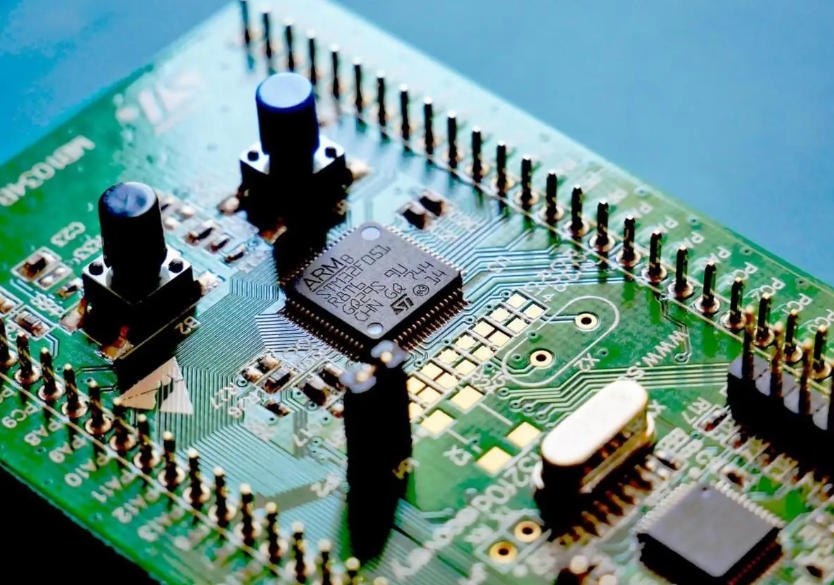
Here’s something nobody tells beginners upfront: the schematic and the physical layout are two completely different disciplines, and you need competence in both. Schematic capture is about electrical connectivity and logical correctness — making sure every pin goes where it should. Board layout is about physical geometry, thermal management, signal integrity, and manufacturability — making sure the board can actually be built, assembled, and operated reliably. Many people strong at one are weak at the other. Budget your learning time accordingly.
Before you open any software: Spend thirty minutes reading the overview section of your target component’s datasheet. Understand what the chip does, what voltage it needs, what package it comes in, and what the pinout looks like. This single habit prevents more beginner mistakes than any other piece of advice in this guide.
Choosing Your EDA Tool
Your EDA (Electronic Design Automation) tool is where you’ll spend hundreds of hours. Choose well, and it becomes invisible — you focus on the design, not the tool. Choose poorly, and every session is a fight with the interface.
Free Options That Are Actually Good
KiCad has become the default recommendation for beginners entering the field in 2026. It’s open-source, fully featured, handles multi-sheet schematics, includes a capable PCB editor, and generates production-quality gerber files. The interface isn’t as polished as commercial alternatives — there’s a learning curve, and some operations take more clicks than they should — but it does everything a professional workflow demands, and there’s never a license fee. The community is large and active: whatever problem you encounter, someone has already solved it and posted the answer.
EasyEDA (by LCSC/JLCPCB) runs entirely in your browser and integrates directly with component sourcing and PCB ordering. The workflow is fast: design your board, click order, receive parts and PCBs together. The trade-off is ecosystem lock-in and some limitations for complex, multi-sheet designs. For simple boards, quick prototypes, and learning the basics, it’s excellent.
Autodesk Fusion 360 Electronics bundles schematic and board design with mechanical CAD — valuable when your PCB needs to interface with a custom enclosure. The free tier covers small boards adequately.
Commercial Options
Altium Designer remains the industry standard for professional work. If you’re heading toward a career in electronics hardware, learning Altium is a worthwhile investment. The subscription is expensive for personal use, but Altium 365 adds cloud collaboration and managed libraries that teams rely on.
Cadence Allegro and Mentor PADS dominate in larger enterprises. You probably won’t need these for personal projects, but they’ll appear if you end up working at an electronics company.
My Recommendation
Start with KiCad. It’s free, it’s capable, and it teaches you proper design methodology without hiding complexity behind an oversimplified interface. If you later need Altium for professional work, the concepts transfer directly — the tools look different, but the underlying process is the same.
Schematic Design: Where Most Mistakes Begin
Here’s an uncomfortable truth that experienced designers learn the hard way: most PCB failures that surface during debug or manufacturing trace back to errors made during schematic capture. Not layout problems — schematic errors. A misplaced resistor value. An unconnected pin. A missing bypass capacitor. The schematic is your source of truth, and inaccuracies here propagate everywhere downstream.
3.1 Organizing Your Schematic
Resist the temptation to cram everything onto one enormous sheet. Use hierarchical sheets to partition your design into functional blocks:
- Power supply and regulation
- Microcontroller and digital peripherals
- Analog signal conditioning
- Connectors, protection, and I/O
Each block gets its own sheet. This makes the schematic readable, debuggable, and reusable across projects. A clean, well-organized schematic is the single most important habit you can develop as a designer.
3.2 Symbols and Footprints: Two Things That Must Match
This distinction trips up nearly every beginner, and getting it wrong is expensive. Your schematic symbol and your PCB footprint are two separate library entries that must be correctly linked:
- The symbol represents electrical function — a resistor, an op-amp, a microcontroller — drawn as a logical box with pins
- The footprint represents the physical package — the actual pad geometry, pin spacing, and body dimensions that determine whether a component fits on your board
A 10kΩ resistor symbol could map to an 0402, 0603, 0805, 1206, or through-hole axial package. If you select the wrong footprint in your schematic library, your layout will contain pads that don’t match the physical part, and you’ll discover the problem only when you try to solder components that don’t fit.
Best practice: After selecting each component, open its footprint in the board editor and physically measure the pad pitch, pad width, and overall dimensions against the mechanical drawing in the datasheet. Fifteen minutes of verification prevents a completely wasted board.
3.3 Net Labels and Power Symbols
Use net labels generously. Tracing a wire across a sprawling schematic to find where it connects is tedious and error-prone. Instead, label the connection point and find its partner by searching for the same label:
+3V3
GND
SDA
SCL
SPI_MOSI
USB_D+
USB_D-
ADC_IN3
Power symbols (VCC, GND, +5V) create implicit connections across sheets. Ensure every power rail has an explicit net label on at least one sheet so you can verify the complete power distribution in your netlist.
3.4 Annotation and Electrical Rules Check
After your schematic looks “finished,” annotate it. Annotation assigns reference designators (R1, R2, C1, U1, J1…) to every component automatically. You can customize the numbering scheme, but sequential is fine for most designs.
Then run an Electrical Rules Check (ERC). The ERC catches:
- Unconnected pins (intentional ones should get a “no connect” flag)
- Multiple drivers on a single net (two outputs fighting each other)
- Missing power connections
- Short circuits between power rails
A clean ERC confirms internal consistency. It doesn’t mean the design is correct — you can still have a resistor where a capacitor should be, or a net connected to the wrong logical point. The ERC is a necessary filter, not a sufficient one. Review the schematic yourself, and if possible, have someone else look over it before moving to layout.
The unconnected pin trap: Modern ICs have dozens or hundreds of pins. Leaving an enable pin floating, a reset pin un-pulled, or a power pin unwired will produce a board that either doesn’t work or behaves erratically. The ERC catches some of these, but not all. Before finalizing, go through every IC’s datasheet pin-by-pin and verify that each pin is connected to the correct net. Tedious work. Absolutely essential work.
3.5 Build Your BOM Early
Don’t wait until layout is complete to assemble your Bill of Materials. Start it during schematic capture. For each component, record the value, package, manufacturer part number, and supplier part number. Then verify availability.
A common beginner failure mode: designing a schematic with generic placeholders, then discovering during procurement that the exact part you need is discontinued, back-ordered for 40 weeks, or costs $8 each at low quantities. Check LCSC, DigiKey, or Mouser while you’re selecting components — not after routing is finished.
3.6 Common Schematic Errors
Patterns that appear repeatedly in beginner designs:
Wrong connector pin numbering. You assumed pin 1 is on the left; the datasheet puts it on the right. Verify against the physical component, not your assumption.
Missing decoupling capacitors. Every IC with a power pin needs at least one bypass capacitor placed as close to the pin as possible. This isn’t optional. One 100nF ceramic cap per power pin is a safe default. Add a bulk capacitor (10µF–47µF) near the power entry point of each circuit section.
Floating digital inputs. I2C lines need pull-ups. Reset pins need pull-ups. Button inputs need defined default states. Every digital input needs to be either driven or pulled to a known level — never left floating.
Regulator capacitor requirements ignored. Every LDO and switching regulator has specific capacitor requirements in its datasheet — capacitance value, ESR range, sometimes specific tested part numbers. Follow the datasheet specifications, not intuition.
No protection on external connections. If your board connects to anything outside — USB ports, antennas, sensors, user-facing headers — it needs ESD protection, current limiting, or voltage clamping. Boards that work on the bench without protection will fail in the field.
Component Selection That Saves You Rework
Choosing the right parts before layout eliminates an entire category of painful redesigns.
4.1 Package Size and Soldering Reality
If you’re hand-assembling your prototype (no reflow oven), package size determines your practical limits:
| Package Type | Pin Pitch | Hand-Soldering Difficulty |
|---|---|---|
| Through-hole (DIP, axial) | 2.54mm | Easy — anyone can do this |
| 0805 passives | N/A | Comfortable with a good iron |
| 0603 passives | N/A | Manageable with practice and magnification |
| SOIC-8/14/16 | 1.27mm | Moderate — flux helps enormously |
| TSSOP | 0.65mm | Challenging — steady hands required |
| QFP (fine pitch) | 0.5mm | Difficult — microscope strongly recommended |
| QFN/DFN (bottom pads) | 0.5mm | Requires hot air rework station |
| BGA | Ball grid | Reflow oven required — not hand-solderable |
For your first boards, stick to through-hole for key components and 0805 for passives. You can always shrink the design later once your assembly skills have caught up with your design ambitions.
4.2 Sourcing and Lifecycle
A part available today might vanish tomorrow. Before finalizing any component in your BOM:
- Check stock across at least two distributors — LCSC, DigiKey, Mouser, or Arrow
- Verify the part isn’t marked NRND (Not Recommended for New Design) or nearing end-of-life
- Check pricing at your expected order quantity — a component at $0.01 per unit in volume may cost $3.00 when buying one
- Look for second-source alternatives in case primary supply runs out
4.3 The Datasheet Is Your Source of Truth
Not the blog post. Not the reference design you found on a forum. The actual datasheet from the manufacturer. Read it completely for every active component in your design. Pay close attention to:
- Recommended operating conditions — voltage range, current limits, temperature range
- Absolute maximum ratings — the thresholds that destroy the part
- Pin descriptions — not just names, but what each pin actually does under different conditions
- Application circuits — these are typically tested and verified by the manufacturer’s engineering team
- PCB layout guidelines — many IC datasheets include these specifically; follow them
A well-chosen component with a thoroughly read datasheet is worth more than an elaborate circuit designed on assumptions.
Board Layout: Getting Physical
Schematic design is electrical engineering. Board layout is electrical engineering combined with spatial reasoning, thermal awareness, and a certain amount of craftsmanship. This is where your abstract design becomes a physical object that a manufacturer can build.
5.1 Board Outline and Layer Stackup
Begin by defining your board outline. If the board fits in an enclosure, measure the internal dimensions, subtract clearances, and draw the outline. Add mounting holes at locations dictated by the mechanical design.
For a typical two-layer board:
Top Layer    — component placement and signal routing
Core         — FR-4 substrate (1.6mm is standard)
Bottom Layer — ground plane and additional routing
Decide early which layer carries your ground reference. For most designs, a ground plane on the bottom layer works well: place components and route signals on top, and use the bottom as a near-continuous copper ground. This provides good signal return paths, reduces electromagnetic interference, and simplifies routing considerably.
5.2 Component Placement
Placement determines 80% of your layout quality. A well-placed board practically routes itself. A poorly-placed board resists every routing decision you make.
Start with the immovable objects. Connectors go at board edges. Mounting holes go where the mechanical design dictates. Large components with thermal or airflow requirements get positioned first. Lock these down and don’t move them.
Group functional blocks together. Decoupling capacitors for your microcontroller go next to the microcontroller. The voltage regulator and its input/output capacitors cluster in their own corner. The analog section stays physically separated from the digital section. Each functional block should form a compact group.
Follow signal flow direction. If signals travel from connector → input filter → ADC → microcontroller → output driver → connector, arrange components in that physical sequence across the board. This minimizes trace lengths and reduces the number of layer changes needed during routing.
Decoupling capacitor placement is critical. “Close” in a schematic sense means nothing. What matters is physical proximity on the board. Place each bypass cap within 2–3mm of the IC power pin it serves, connected with short, wide traces. The parasitic inductance of a long trace between the capacitor and the pin defeats the purpose of having the capacitor there.
Spread out heat-generating components. Don’t cluster your voltage regulator, power transistor, and LED driver in one corner. Thermal load compounds. Separate high-dissipation components and provide adequate copper area for heat spreading.
5.3 Routing Power First
Route your power traces before signal traces. Power paths need width (to carry current without excessive heating) and directness (to minimize voltage drop). Getting them out of the way early prevents the situation where you’ve routed all your signals and now have no room left for adequate power distribution.
Trace width depends on current, copper weight, and acceptable temperature rise. For a quick reference on a 1oz copper, two-layer board with external traces:
| Current | Minimum Trace Width |
|---|---|
| 0.5A | 10 mil (0.25mm) |
| 1A | 20 mil (0.5mm) |
| 2A | 50 mil (1.27mm) |
| 3A | 100 mil (2.54mm) |
These are conservative estimates for traces in open air. Internal copper layers dissipate heat less effectively and require wider traces for equivalent current capacity. Use an IPC-2221 trace width calculator for precise values given your specific conditions.
5.4 Ground Plane Strategy
Instead of routing ground as individual traces everywhere, dedicate one layer to a solid copper pour connected to ground. Components and vias tie into this plane. The benefits are substantial: reduced ground impedance, improved signal return paths, better EMI performance, and simpler routing overall.
If you must route a signal trace through the ground plane (creating a gap in the copper), keep the gap as narrow as possible and never create isolated ground islands — sections of copper with no connection to anything. Isolated copper acts as an antenna, radiating noise.
For designs with both analog and digital sections, keep the ground plane continuous rather than splitting it. Connect analog and digital grounds at a single point near the ADC or wherever the domains interface. Chopped ground planes create more problems than they solve in most designs.
5.5 Signal Routing Principles
For signals running at frequencies above a few megahertz, a few routing habits make the difference between a board that works and one that radiates noise:
- Keep traces short — every millimeter adds inductance and potential for coupling
- Avoid running sensitive signals parallel to noisy ones for long distances — crosstalk scales with parallel run length
- Route high-speed signals directly over a continuous ground plane — return current follows the path of least inductance, which is directly beneath the signal trace
- Match trace lengths for differential pairs (USB D+/D-, LVDS) — mismatch converts differential signals to common-mode noise
- Use 45-degree or curved corners instead of right angles — sharp corners create impedance discontinuities and can trap etchant during manufacturing
- Don’t run critical traces underneath components you can’t easily remove during debugging
5.6 Via Management
Vias connect traces between layers. Standard manufacturing minimums vary by fab house, but typical capabilities for a standard two-layer board:
| Parameter | Conservative | Typical |
|---|---|---|
| Minimum drill diameter | 0.3mm (12mil) | 0.2mm (8mil) |
| Minimum annular ring | 0.25mm (10mil) | 0.15mm (6mil) |
| Minimum via pad diameter | 0.8mm (32mil) | 0.5mm (20mil) |
For prototyping and hand-soldering, go larger than minimum. Use 0.3mm drill with 0.7mm pad diameter as your default. You’ll appreciate the margin when you need to probe a via during debug or rework a connection.
5.7 Copper Pour and Thermal Relief
Adding copper pour (ground fill) to unused board area is standard practice. It reduces ground impedance, distributes thermal load, and creates a more uniform etching process.
One critical detail: when a through-hole pad connects to a large copper pour, it should use a thermal relief pattern — thin spoke connections instead of solid copper. Without thermal relief, the copper plane acts as a massive heat sink during soldering, making it nearly impossible to get the joint hot enough for the solder to flow. Most EDA tools apply thermal relief by default, but verify that the setting is active. Surface-mount pads on internal layers connected to pours may not get thermal relief automatically — check these manually.
Design Rules, DRC, and Why They Matter
Design rules are the physical constraints your EDA tool enforces during layout. They represent the manufacturing limits of your chosen fabrication process. Set them to match your manufacturer’s actual capabilities — not guesses, not defaults from a different fab house, and not the tightest numbers you’ve seen somewhere online.
6.1 Setting Up Design Rules
Get the specification sheet from your intended PCB manufacturer and enter those exact values as your design rules. For a standard two-layer board, here’s a reasonable range:
| Parameter | Conservative (Safe) | Typical | Advanced |
|---|---|---|---|
| Min trace width | 0.25mm (10mil) | 0.15mm (6mil) | 0.1mm (4mil) |
| Min trace spacing | 0.25mm (10mil) | 0.15mm (6mil) | 0.1mm (4mil) |
| Min drill diameter | 0.3mm (12mil) | 0.2mm (8mil) | 0.15mm (6mil) |
| Min annular ring | 0.25mm (10mil) | 0.15mm (6mil) | 0.1mm (4mil) |
| Min hole-to-hole | 0.3mm (12mil) | 0.25mm (10mil) | 0.15mm (6mil) |
| Min copper-to-edge | 0.3mm (12mil) | 0.2mm (8mil) | 0.15mm (4mil) |
| Min silkscreen width | 0.2mm (8mil) | 0.15mm (6mil) | 0.1mm (4mil) |
For your first several boards, use the conservative column. The small sacrifice in routing density is worth the dramatic improvement in manufacturing yield and personal sanity.
6.2 Running DRC
After routing is complete, run Design Rule Check. This validates every trace, via, pad, and copper pour against the constraints you defined. It catches:
- Traces too close together (potential shorts during manufacturing)
- Traces narrower than the fab can reliably produce
- Vias too close to pads or other vias
- Copper too close to the board edge (routed away during profiling)
- Silkscreen overlapping solder pads (gets clipped during manufacturing)
- Unconnected nets (broken circuits)
Fix every DRC error before generating manufacturing files. Every single one. A clearance violation that seems minor on screen can produce a microscopic solder bridge on the physical board. An unrouted net means a connection that simply doesn’t exist in hardware.
6.3 ERC and DRC Are Complementary
DRC catches physical violations. ERC catches electrical violations. A board can pass DRC with zero errors and still be electrically incorrect if schematic mistakes were missed. Run both checks. They test different dimensions of design correctness.
7. Generating Gerber and Drill Files
Gerber files are the universal format for communicating PCB designs to manufacturers. Each file describes one layer of the board as a series of drawing commands — lines, arcs, flashes, and apertures. Your EDA tool generates them automatically from your layout.
7.1 File Map for a Standard Two-Layer Board
| File | Content |
|---|---|
| F.Cu | Top copper layer — traces, fills, pad connections |
| B.Cu | Bottom copper layer |
| F.Mask | Top solder mask openings — where green coating is removed to expose pads |
| B.Mask | Bottom solder mask openings |
| F.Silk | Top silkscreen — component outlines, reference designators, logos |
| B.Silk | Bottom silkscreen (if used) |
| F.Paste | Top solder paste stencil openings (needed for SMT assembly) |
| B.Paste | Bottom solder paste stencil openings (rare for simple boards) |
| Edge.Cuts | Board outline — defines the physical board shape |
| Drill | NC Excellon drill file — hole positions, sizes, and plating info |
7.2 Generating in KiCad
Go to File → Fabrication Outputs → Gerbers. Select the layers appropriate for your board (for a basic two-layer board, that’s F.Cu, B.Cu, F.Mask, B.Mask, F.Silk, Edge.Cuts). Set your output directory, choose the Gerber X2 or RS-274X format, and generate.
Then go to File → Fabrication Outputs → Drill Files. Set the format to Excellon, units to metric (mm), and coordinates to absolute. Generate.
Zip all gerber files and the drill file into a single archive. This is what you upload to your manufacturer.
7.3 Verifying Gerbers Before Sending
This step catches errors that save you from wasting an entire production cycle. After generating gerbers, open them in a dedicated viewer before uploading to the fab:
- KiCad Gerber Viewer — built in, good for quick checks
- PCBWay’s online viewer — upload and preview the manufactured result
- JLCPCB’s online viewer — same function, different interface
- Gerbv — lightweight open-source standalone viewer
Check for these common issues:
- Board outline forms a closed contour (no gaps)
- Copper on each layer matches what you see in the PCB editor
- Solder mask openings appear on every pad that needs soldering
- Drill hits are present and in correct locations
- Silkscreen text is readable and doesn’t overlap pads
- No unexpected copper artifacts or stray features
Five minutes of gerber review prevents five days of waiting for corrected boards.
Preparing Your Files for the Fab House
Good gerbers are necessary but not complete. Clear communication with your manufacturer prevents costly misunderstandings.
8.1 What to Specify in Your Fab Notes
Include a text document or fill in the manufacturer’s online order form with these details:
Board basics
- Dimensions: length × width × thickness (e.g., 80mm × 50mm × 1.6mm)
- Layer count: 2, 4, 6, etc.
- Copper weight: per layer (1oz / 35µm is standard for both layers on a two-layer board)
- Material: FR-4 Tg130 for standard; FR-4 Tg170 for lead-free assembly thermal profiles
Finish and coating
- Surface finish: HASL (lead-free) for prototyping, ENIG for fine-pitch components
- Solder mask color: green is cheapest and fastest; other colors may add cost and lead time
- Silkscreen color: white on green mask is standard
Special requirements
- Controlled impedance: only for high-speed designs — specify target impedance and which nets require it
- Via treatment: tented (mask-covered), plugged, or left open
- Panelization: specify if you need multiple copies arranged on a single panel
8.2 Common Fab Note Mistakes
Specifying impedance control unnecessarily. Impedance-controlled routing costs more and requires tighter manufacturing tolerances. If your design runs at DC through a few MHz, you almost certainly don’t need it.
Omitting the surface finish specification. If you don’t specify, most fabs default to HASL. That works for through-hole and coarse-pitch SMT, but creates uneven pad surfaces that cause solder bridging on fine-pitch QFN and BGA packages. Specify ENIG when using those packages.
Forgetting board thickness. 1.6mm is the standard default, but confirm it. Some fabs default to 1.0mm or 1.2mm for certain layer counts, which changes mechanical fit in enclosures designed for 1.6mm boards.
Understanding PCB Specifications
Familiarity with the terminology your manufacturer uses helps you make informed decisions and communicate without ambiguity.
9.1 Layer Count
| Layers | Typical Application |
|---|---|
| 1 (single-sided) | Very simple circuits, cost-sensitive consumer products |
| 2 (double-sided) | Most prototyping, medium-complexity designs |
| 4 | Designs with power/ground planes, moderate signal density |
| 6–8 | High-density designs with fine-pitch BGAs and many nets |
| 10+ | Complex digital systems, backplanes, computing hardware |
For your first boards, two layers is plenty. Move to four when you have a specific technical reason — not because it sounds more professional.
9.2 Copper Weight
| Weight | Thickness | Typical Use |
|---|---|---|
| 0.5oz | 17µm | Fine-pitch signal routing where density matters |
| 1oz | 35µm | Standard — good balance of current capacity and routability |
| 2oz | 70µm | Power circuits, motor drivers, high-current applications |
| 3oz+ | 105µm+ | Dedicated power boards, high-current converters |
The trade-off is real: heavier copper handles more current, but etching fine features becomes significantly harder. A 10-mil trace with 2oz copper is much more difficult to manufacture cleanly than the same trace with 1oz.
9.3 Surface Finish Comparison
| Finish | Advantages | Disadvantages | Best For |
|---|---|---|---|
| HASL (lead-free) | Cheapest, widely available, excellent solderability | Uneven surface, not ideal for fine-pitch | Prototyping, through-hole, coarse SMT |
| ENIG | Flat surface, long shelf life, good for fine-pitch | More expensive, nickel barrier layer | QFN, BGA, fine-pitch SMT |
| OSP | Flat, inexpensive, lead-free compatible | Short shelf life (~6 months) | High-volume production with fast assembly |
| Immersion Silver | Flat, good for high-frequency signal integrity | Tarnishes over time | RF and high-frequency applications |
| Hard Gold | Extremely durable, resists wear | Very expensive | Edge connectors, switch contacts |
9.4 Manufacturing Tolerances
PCB fabrication has inherent variability. Know these numbers so you’re not surprised by the physical board:
| Feature | Typical Tolerance |
|---|---|
| Trace width | ±20% of nominal |
| Drill diameter | ±0.1mm |
| Drill-to-copper registration | ±0.15mm |
| Board dimensions | ±0.2mm |
| Copper thickness | ±20% of nominal |
| Solder mask annular ring | ±0.05mm |
These tolerances stack. A trace could be 20% narrower while shifted 0.15mm from its nominal position, adjacent to another trace that’s 20% wider. Design rules are calculated to accommodate worst-case stacking — which is exactly why you should respect them rather than pushing limits on your first design.
Prototype vs. Production: When to Commit
There’s a meaningful difference between a prototype board and a production board, and understanding the transition saves money and avoids painful redesigns at the worst possible time.
10.1 The Prototype Phase
Prototypes exist to validate your design. You’re answering questions: Does the circuit work as intended? Are there layout-related problems — noise coupling, thermal issues, impedance mismatches? Do all components fit and can they be assembled reliably?
For prototyping:
- Order small quantities — 5 to 10 boards is typical and cost-effective
- Use standard specifications — 1.6mm, 2-layer, 1oz, HASL, green solder mask
- Prioritize fast turnaround over per-unit cost savings
- Single boards are fine — panelization isn’t necessary
Prototype pricing from most online fabs for a simple two-layer board (50mm × 50mm, 5 pieces) runs $2–20 depending on the manufacturer. This is remarkably affordable. There’s no excuse for skipping the prototype stage to save a few dollars.
10.2 When You’re Ready for Production
Move from prototype to production when all of the following are true:
- The board has passed functional testing in its intended environment (not just on the bench)
- You’ve completed at least two prototype iterations for anything beyond the simplest designs
- All component availability has been confirmed for your production timeline
- The enclosure and mechanical interface have been finalized — no more dimensional changes
- The BOM cost at production volume is acceptable
For production runs:
- Panelize your boards for efficient handling and assembly
- Add fiducial marks — alignment dots that pick-and-place machines use for optical registration
- Specify panel breakaway method — V-score for straight cuts, tab routing for perforated tabs
- Request first-article inspection — detailed measurements and photographs of the first production run
- Lock down the BOM — no substitutions, no last-minute changes
Don’t transition too early. A design change during prototyping costs you the price of another small batch — trivial compared to the alternatives. A design change after entering production is expensive, slow, and painful.
Common Beginner Mistakes and How to Avoid Them
Compiled from years of reviewing designs, debugging boards, and watching what goes wrong. Experienced designers make these mistakes too — they just make them less often.
Mistake 1: Not Reading the Datasheet
You design a circuit based on a reference schematic from a blog, but the blog used a different IC variant. The pinout is slightly different. Your board doesn’t work. You spend a week debugging before discovering the mismatch.
Fix: Verify every pin assignment against the datasheet of the exact part in your BOM. Not a similar part. Not the one in the tutorial. The specific part you’re ordering.
Mistake 2: Missing Decoupling Capacitors
Your microcontroller resets randomly. Your op-amp oscillates. Your regulator output has excessive ripple. Hours of debugging lead to the same conclusion every time: the bypass caps are missing or poorly placed.
Fix: One 100nF ceramic cap within 3mm of every IC power pin. A 10–47µF bulk cap near each regulator output. Follow the IC manufacturer’s specific recommendations — some parts require multiple caps of different values.
Mistake 3: Routing Without a Ground Reference
Signals pick up noise. The board passes bench testing but behaves unreliably in its application or fails EMC testing.
Fix: Maintain a solid ground plane. Route critical signals directly above it. Avoid routing over splits or gaps in the ground plane. Every signal needs a continuous return path directly beneath it.
Mistake 4: Using Minimum Trace Width for Power
Power traces overheat. Inductive impedance on long thin traces causes voltage drop and noise. The board works at room temperature but fails in warm environments.
Fix: Calculate trace widths based on actual current. Use wider traces for power distribution. Refer to the trace width guidelines in Section 5.3 and the IPC-2221 standard for precise calculations. When in doubt, go wider — copper is cheap.
Mistake 5: Skipping DRC
You send gerbers to the fab. Two weeks later, the boards arrive. A trace has a microscopic gap to an adjacent pad. There’s a solder bridge you can barely see with a magnifying glass. The board shorts.
Fix: Run DRC with your manufacturer’s specs as the rule set. Fix every error. Run it again to confirm your fixes didn’t introduce new violations. No exceptions.
Mistake 6: Silkscreen Overlapping Pads
Silkscreen ink on a solder pad prevents proper wetting during assembly. The component doesn’t solder correctly, or the joint is mechanically weak.
Fix: Run silkscreen DRC after completing layout. Check that no text or graphic elements overlap exposed copper pads. Verify that silkscreen is readable — not upside-down, not cut off by the board edge, not obscured by nearby components.
Mistake 7: Wrong Footprint Selected
You placed an SOIC-8 in the schematic, but the footprint library entry is actually an MSOP-8 with narrower pitch. The pads don’t match the physical IC. The board is useless for that component.
Fix: After selecting each component, open its footprint in the PCB editor. Measure pad pitch, pad width, pad length, and body dimensions against the datasheet mechanical drawing. Five minutes per component prevents a wasted board.
Mistake 8: Forgetting Assembly Constraints
All your SMT components ended up on the bottom layer. You planned to hand-assemble, but now you need reflow — which means the top-side components fall off in the oven.
Fix: Place SMT components on the top layer. Put through-hole components on the bottom. If both sides need SMT, plan the assembly sequence carefully and discuss with your manufacturer before finalizing the layout.
Mistake 9: No Thermal Relief on Copper Pour Connections
A through-hole pad connects directly to a solid copper plane. During soldering, heat wicks into the plane instantly and the joint never reaches temperature.
Fix: Use thermal relief patterns (thin spoke connections) on through-hole pads connected to copper pours. Most EDA tools do this automatically — verify the default settings are active. SMT pads on internal layers may need manual thermal relief addition.
Mistake 10: Skipping the Prototype Entirely
“I’m confident this works. Let me order 100 boards.” The boards arrive. Something doesn’t work. You have 100 useless boards and need to redesign anyway.
Fix: Always prototype first. Even if you’re 99% confident. Especially if you’re 99% confident. That misplaced confidence is usually the problem. Five prototype boards cost a fraction of what a production run costs, and they’ll catch the errors that simulations, reviews, and staring at the screen missed.
A Realistic Learning Path
If you’re starting from zero, here’s a progression that builds competence incrementally. Each stage produces something tangible — a board you can hold, test, and learn from.
Weeks 1–2: Foundations
- Download KiCad and work through the official Getting Started tutorial
- Schematic: draw a simple circuit — LED with a current-limiting resistor and a switch
- Layout: route the simplest possible board — two components, two traces, no vias
- Generate gerbers and open them in a viewer to confirm they look correct
- Order the board ($2–5 for five pieces from most online fabs)
- When it arrives, solder the components and verify it works
That first board — even if it’s just an LED that lights up when you flip a switch — teaches you the complete workflow end-to-end. Nothing else substitutes for this experience.
Weeks 3–4: Building Complexity
- Design a slightly more complex circuit: a 555 timer, an Arduino shield, or a USB-to-serial adapter
- Use both copper layers
- Mix through-hole and surface-mount components
- Practice decoupling capacitor placement and power trace routing
- Solder the board by hand — learn where your personal soldering limits are
- Debug: if something doesn’t work, trace the problem systematically rather than randomly reflowing joints
Month 2: Intermediate Design
- Design a board with a microcontroller (STM32, ESP32, or ATmega family)
- Use hierarchical schematics to organize a multi-sheet design
- Implement a ground plane and learn how it changes your routing approach
- Work with finer-pitch packages (SSOP, TQFP) and practice soldering them
- Add test points for signal probing during debug
- Design for a specific enclosure — measure first, then route to fit
Month 3 and Beyond
- Design a four-layer board and understand when the extra layers are justified
- Work with USB 2.0 or 10/100 Ethernet — these require attention to controlled impedance basics
- Design for automated assembly: pick-and-place, reflow, stencil design
- Explore signal integrity concepts for high-speed digital design
- Contribute to open-source hardware projects for community feedback on your designs
- Start a personal design journal — document what went wrong and why, so you don’t repeat mistakes
The Most Important Advice in This Entire Guide
Design a board. Build it. Test it. Find your mistakes. Then design the next one better. No amount of reading, watching tutorials, or studying reference designs substitutes for the experience of debugging a physical board that doesn’t work and figuring out why. Every experienced PCB designer has a drawer full of failed boards. That drawer is their education.
Frequently Asked Questions
How much does it cost to get a PCB manufactured?
For a standard two-layer board (50mm × 50mm, 1.6mm thick, 1oz copper, green solder mask, HASL finish), expect $2–20 for 5–10 pieces from online prototype fabs. Four-layer boards cost roughly two to three times more. Per-unit cost drops significantly at volume — a production run of 1,000 boards might cost $0.50–2.00 per board depending on size, layer count, and special requirements.
How long does PCB manufacturing take?
Prototype orders typically ship in 1–3 business days for standard specifications, plus 2–7 days for shipping depending on your location and carrier. Rush services can deliver in 24 hours at a premium. Production orders for larger quantities may take 5–10 business days.
What software is best for PCB design as a beginner?
KiCad is the strongest starting point for most beginners in 2026. It’s free, fully capable, and teaches proper design methodology. EasyEDA works well if you want a streamlined design-to-order workflow. Fusion 360 Electronics is worth considering when you need mechanical CAD integration for enclosure design.
Can I make a PCB at home?
Yes, using methods like toner transfer or photoresist etching. Home-fabricated boards are limited to simple single or two-layer designs with minimum feature sizes around 0.3mm. For anything beyond the most basic circuits, professional manufacturing is affordable, faster, and produces far more reliable results with finer tolerances.
What is gerber format and why do manufacturers use it?
Gerber is a vector file format that describes each layer of a PCB as a series of drawing commands — lines, arcs, and aperture flashes. It’s been the industry standard since the 1960s because it’s simple, well-specified, and every PCB manufacturing system worldwide can interpret it. Your EDA tool generates gerber files from your completed layout; the manufacturer’s CAM software reads them to drive fabrication equipment.
Should I use through-hole or surface-mount components?
For beginners, a hybrid approach works best. Use through-hole for components you’ll connect, disconnect, and probe frequently — connectors, headers, switches, large capacitors. Use 0805 surface-mount packages for passive components — resistors and capacitors that stay put once soldered. This lets you practice SMT techniques on the easiest packages while keeping interactive components accessible for hand work.
What happens if my PCB design has errors?
If errors are caught during the manufacturer’s review process, they may contact you before fabrication begins — but not always. Some fabs build exactly what the gerber files specify, errors included. Common consequences of design errors include short circuits, open circuits, misaligned drills, and unrouted connections. This is exactly why gerber review, DRC, and careful verification are non-negotiable steps — fixing an error on your computer costs nothing; fixing an error on 100 manufactured boards costs everything.
What’s the difference between a prototype and production PCB?
A prototype board is made in small quantities with standard specifications and fast turnaround, designed to validate your circuit design and catch problems early. Production boards are made in larger quantities with customized specifications — panelization, specific surface finishes, assembly instructions, testing — and optimized for efficient high-volume assembly. The electrical design is the same; the manufacturing process, quality controls, and documentation requirements differ substantially.
How do I know my design is ready to send to a manufacturer?
Run through this checklist before uploading gerbers:
- DRC passes with zero errors using your manufacturer’s specification as design rules
- ERC passes with zero errors
- All nets are routed — no unrouted connections remain
- Gerbers generated and visually verified in a gerber viewer
- Board outline forms a closed contour with no gaps
- Drill file generated with correct format, units, and coordinates
- BOM complete with valid manufacturer part numbers and confirmed availability
- Fab notes specify all critical parameters — layers, thickness, copper weight, surface finish, mask color
- One final comparison between the gerber viewer output and your PCB editor layout
Do I need to learn soldering before designing PCBs?
You don’t strictly need to solder in order to design a PCB, but understanding soldering constraints makes you a substantially better designer. Knowing the minimum package size you can reliably hand-solder, recognizing how thermal relief affects assembly, and understanding automated assembly limitations all feed directly into better layout decisions. If possible, learn basic soldering alongside your PCB design education — the two skills reinforce each other.
This guide covers the fundamentals of PCB design from first principles through manufacturing handoff. For specific design questions, manufacturing specifications, or a review of your files before ordering, our engineering team is available to provide feedback and recommendations.
Email:[email protected]



0 Comments