




A PCB does not need to look polished to accept solder, but its exposed pads must be free of loose debris, fingerprints, grease, and other contamination that can interfere with wetting. The safest approach is to inspect first, identify what is actually on the board, and use the least aggressive cleaning method that works.
For many newly fabricated boards that were packaged and stored correctly, preparation may be as simple as handling the edges, removing loose dust, and checking the pads. Older boards, hand-etched boards, and repair boards may need more work. This guide explains how to clean a PCB before soldering without treating every surface problem as the same.
Do You Need to Clean a PCB Before Soldering?
Start with a close visual inspection under bright light. A clean, recently manufactured PCB with an intact surface finish may not need solvent cleaning. Unnecessary scrubbing can introduce lint, static, scratches, or new contamination. Clean the board when you can see or reasonably expect fingerprints, oil, dust, adhesive residue, old flux, or light tarnish on the areas to be soldered.
The board type changes the decision:
- New fabricated PCB: inspect the pads and packaging condition. Avoid touching exposed contacts. Use only light cleaning if contamination is present.
- Bare DIY copper board: remove fabrication debris and deal with surface oxidation carefully before applying flux and solder.
- Repair or rework board: disconnect all power, identify coatings and sensitive components, and separate old flux cleanup from preparation of the specific joint.
Cleaning cannot restore missing copper, lifted pads, deeply corroded conductors, or a surface finish that has deteriorated beyond use. Those conditions require repair, process review, or board replacement rather than stronger scrubbing.
What You Need to Clean a PCB Safely
Set up a clean, well-lit, ventilated workspace. Use ESD controls appropriate for the board and its components. Disconnect the board from every power source and remove batteries where practical. Isopropyl alcohol and many electronics cleaners are flammable, so keep them away from soldering irons, hot-air tools, sparks, and open flames until the liquid and vapors have fully dispersed.
| Item | Purpose | Caution |
|---|---|---|
| Soft ESD-safe brush | Loosens dust and light surface contamination | Use gentle pressure; a hard brush can scratch coatings or catch small parts |
| Lint-free wipes or foam swabs | Lifts dissolved contamination away from pads | Replace them as they become dirty so residue is not spread |
| Electronics-grade cleaner or high-purity IPA | Removes many oils and light residues | Check compatibility with the PCB, markings, plastics, adhesives, and components |
| Magnification and bright light | Reveals fibers, corrosion, coating damage, and pad condition | Visual inspection does not measure ionic cleanliness |
| Gloves or finger cots | Prevents fresh fingerprints on cleaned pads | Use clean, powder-free products suitable for electronics work |
Use the cleaner recommended by the flux, solder paste, board, or component manufacturer when such guidance is available. A familiar solvent is not automatically compatible with every connector, display, switch, label, conformal coating, or adhesive.
Choose the Cleaning Method by Contaminant
Cleaning works best when the method matches the soil. Begin with the mildest action and escalate only when inspection shows it is necessary.
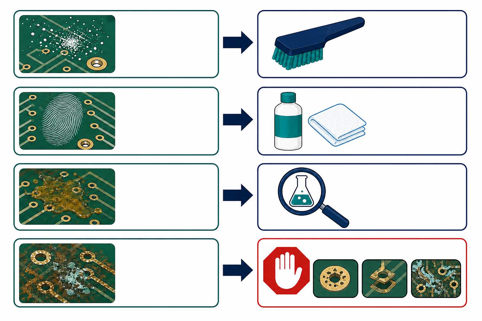
| Condition | First action | If it remains | Stop condition |
|---|---|---|---|
| Loose dust or fibers | Use a clean, soft ESD-safe brush or suitable controlled air | Inspect under magnification | Stop if air pressure could damage parts or drive debris into connectors |
| Fingerprints or light oil | Use a small amount of compatible electronics cleaner on a lint-free wipe or swab | Repeat with a fresh wipe, then dry fully | Stop if ink, plastic, adhesive, or coating reacts |
| Unknown sticky residue | Identify its source and check the material or process data | Use the specified cleaner | Do not experiment with aggressive household solvents on the assembly |
| Light tarnish on exposed copper | Confirm the pad finish and assess the affected area | Use only controlled, localized treatment appropriate to that finish | Stop at pitting, lifting, missing plating, or widespread corrosion |
| Old flux on a repair board | Follow the flux manufacturer’s cleaning chemistry | Remove dissolved residue with clean wipes rather than letting it redeposit | Stop if liquid can enter unsealed switches, displays, microphones, or connectors |
If the PCB has a conformal coating, cleaning alone will not expose a solderable pad. Coating removal is a separate controlled repair operation. Review the risks before attempting to remove solder mask or protective coating near copper.
How to Clean a PCB Before Soldering: Step by Step
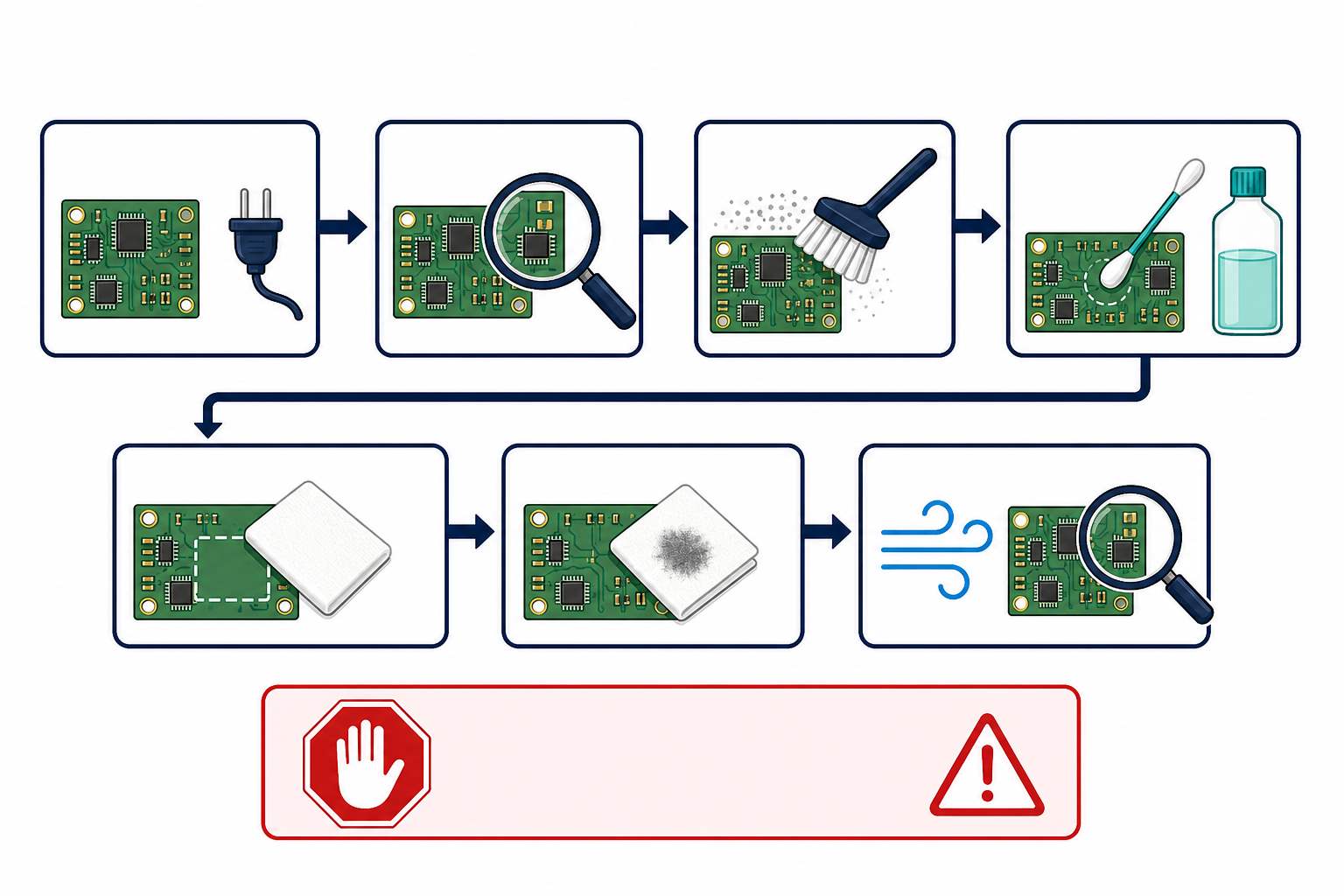
- Isolate the board. Disconnect power, remove batteries where possible, and allow charged circuits to discharge according to the equipment’s service procedure.
- Identify the board condition. Determine whether it is a new bare board, a DIY copper board, or a populated repair assembly. Look for coatings, corrosion, lifted pads, and liquid-sensitive parts.
- Remove loose debris. Hold the PCB by its edges and gently brush away dust and fibers. Do not use your fingers to test whether a pad feels clean.
- Test compatibility. Check manufacturer guidance. If compatibility is uncertain, test the cleaner on a noncritical area or a representative spare material before treating the soldering area.
- Apply cleaner sparingly. Moisten a lint-free wipe, foam swab, or suitable brush instead of flooding the board. Work on a small area at a time.
- Lift contamination away. Agitate gently, then collect the dissolved material with a fresh wipe. Allowing dirty solvent to evaporate on the PCB can simply move contamination to the edge of the cleaned area.
- Repeat only if needed. Use a clean applicator for the second pass. If the surface does not improve, stop and reconsider the contaminant and cleaner instead of applying more force.
- Dry the board completely. Follow the cleaner manufacturer’s drying instructions. Pay attention to vias, connectors, sockets, and spaces under components where liquid can remain trapped.
- Inspect again. Under magnification, check that the pads are intact, free of fibers and visible film, and ready for flux and solder.
Once the board is ready, use correct soldering temperature, flux, tip condition, and dwell time. Cleaning cannot compensate for a contaminated iron tip or incorrect technique. See the separate step-by-step guide to soldering on a PCB for the next stage.
How to Handle Tarnished or Oxidized Pads
Oil dissolving and oxide removal are different tasks. Solvent may remove grease but will not necessarily restore a degraded metal surface. First determine whether you are looking at bare copper, HASL, ENIG, OSP, immersion tin, or another finish. Each finish has different storage and handling limits. The overview of PCB durability and surface-finish aging explains why oxidation resistance varies.
For a small bare-copper DIY pad with superficial tarnish, a very gentle, localized mechanical treatment may expose a solderable surface. This is not a general recommendation for plated production boards. Aggressive erasers, fiberglass tools, knives, or abrasive pads can thin or remove the finish, scratch solder mask, cut traces, and leave debris. Stop if the copper is pitted, the pad moves, the finish flakes, or corrosion extends under the mask.
If a new production board has widespread solderability problems, preserve samples and contact the fabricator or assembler. Document storage time, packaging, finish, affected locations, flux, thermal profile, and solder alloy. That evidence is more useful than polishing every pad and destroying the original condition.
Engineering Scenario: Cleaning a Misprinted PCB Before Rework
An IPC-hosted technical paper describes a designed experiment for cleaning misprinted PCBs before downstream assembly work. The study did not assume that one cleaner would work for every board. It evaluated wet solder paste, SMT adhesive, reflowed residues, and several chemistry families on two test vehicles: a single-sided 3 by 5 inch PCB and a double-sided 5 by 8 inch PCB. The boards included high-temperature OSP and immersion-silver finishes.
The team deliberately tested cleaning delays of zero, two, and four hours. It assessed the same locations under 40x magnification and also used ionic-residue measurements. One reason for including OSP boards was to observe whether cleaning removed or degraded the protective finish, because that could affect later soldering. The paper reported that the best process in that experiment depended on the target residue, cleaning equipment, and chemistry; its stated optimum was not presented as a universal bench-cleaning recipe.
The practical lesson is directly relevant before soldering: classify the contamination and identify the surface finish before choosing a process. A method that removes paste but damages OSP, spreads residue, or leaves hidden ionic contamination has not prepared the board successfully. For production problems, preserve evidence and validate the process on representative boards rather than increasing solvent strength by trial and error. See the IPC-hosted cleaning-agent evaluation paper for the original experiment, variables, measurements, and limitations.
What Not to Use on a PCB
- Do not clean a powered board. Liquids and energized circuits create shock, short-circuit, and damage risks.
- Do not use an unknown aggressive solvent. Acetone and other strong solvents can attack plastics, coatings, adhesives, and markings.
- Do not soak a populated assembly without a validated process. Liquid can enter switches, relays, connectors, displays, microphones, and other parts that are difficult to dry.
- Do not use shedding tissues or dirty swabs. Fibers and redistributed residue defeat the purpose of cleaning.
- Do not scrape plated pads just to make them shiny. Appearance is not a valid reason to remove protective finish.
- Do not start soldering while solvent remains. Wait until the board and trapped spaces are fully dry and vapors have cleared.
How to Know the PCB Is Ready for Soldering
Before switching on the iron, confirm the following:
- The intended pads are visible and intact, with no lifted edges or missing copper.
- No loose dust, brush bristles, wipe fibers, or visible oily film remains.
- No cleaner is pooled in holes, sockets, connectors, or beneath components.
- The PCB has dried for the time and under the conditions specified for the cleaner and assembly.
- The work area no longer contains flammable liquid or concentrated vapor near heat or sparks.
- The component, flux, solder alloy, and thermal process are suitable for the board finish.
These checks establish practical readiness for bench soldering; they do not certify ionic cleanliness for high-reliability production. Manufacturing acceptance may require a controlled cleaning process and appropriate cleanliness testing. If you need fabrication and assembly support rather than bench rework, review PCBtry’s PCB manufacturing and assembly services.
Pre-Solder PCB Cleaning Checklist
Print this section or save the page with your work notes. It is a general bench-readiness aid, not a cleanliness certificate or a substitute for the PCB, component, flux, cleaner, or equipment manufacturer’s process requirements.
- ☐ All external power sources are disconnected, and battery risk has been addressed.
- ☐ The board is classified as new fabricated, bare DIY copper, or populated repair hardware.
- ☐ The contamination is identified, or the unknown condition has been marked for escalation.
- ☐ The pad finish, coatings, adhesives, plastics, and liquid-sensitive components have been considered.
- ☐ The selected cleaner and tools are compatible with the materials present.
- ☐ Loose debris was removed before liquid cleaner was applied.
- ☐ Cleaning was limited to the necessary area and stopped if a material reacted.
- ☐ Dissolved contamination was lifted with fresh material rather than left to dry on the PCB.
- ☐ No loose fibers, brush bristles, visible film, pooled cleaner, or trapped liquid remains.
- ☐ Pads, traces, vias, and solder mask were inspected for lifting, pitting, corrosion, or missing material.
- ☐ The PCB is fully dry according to the applicable cleaner and component guidance.
- ☐ Flux, solder alloy, tip condition, temperature, and the next soldering step are ready.
Common PCB Cleaning Mistakes
The board looks streaky after IPA. The solvent may have dissolved contamination without removing it. Use a fresh lint-free wipe to lift the liquid and soil away, and avoid cleaning a large area with one dirty swab.
Solder still beads or refuses to wet. The problem may be oxide, damaged finish, insufficient flux, incorrect heat, incompatible solder, or poor tip condition rather than remaining grease. Stop escalating the solvent and diagnose the soldering system.
Silkscreen or plastic becomes cloudy. The cleaner may be incompatible with that material. Stop, prevent further exposure, and consult the relevant material or component instructions.
Residue returns after drying. Contamination may be trapped beneath a component or inside a connector, or the cleaner may not match the residue chemistry. A validated professional process may be required.
A pad starts to lift or change color. Stop brushing or scraping immediately. Heat damage, corrosion, or mechanical damage needs inspection and possibly a repair; further cleaning may make it worse.
Frequently Asked Questions
Should I clean every new PCB before soldering?
No. A recently fabricated PCB that is clean, correctly packaged, and properly stored may need only inspection and careful handling. Clean only when dust, fingerprints, oil, residue, or another relevant condition is present.
Can I use isopropyl alcohol to clean a PCB before soldering?
IPA is commonly used for many light oils and residues, but it is not suitable for every contaminant or every assembly material. Check the board, component, coating, adhesive, and cleaner instructions before use.
Is 70% IPA suitable for PCB cleaning?
Its higher water content usually means slower drying than high-purity IPA. Suitability depends on the contamination, drying process, assembly materials, and product requirements. Use electronics-grade material and follow the applicable process guidance.
Can I clean a PCB with water before soldering?
Some manufacturing processes use deionized water with compatible water-soluble chemistry and controlled drying. That does not make uncontrolled tap-water washing appropriate for every PCB, especially a populated repair board.
Can I use acetone on a PCB?
Do not assume acetone is board-safe. It can attack some plastics, coatings, adhesives, and markings. Use a cleaner explicitly compatible with the materials present.
Should I sand oxidized PCB pads?
Not as a routine method. Abrasion can remove thin surface finish or copper and can damage adjacent solder mask. Identify the finish and condition first; stop and seek repair guidance for pitting, lifting, or widespread corrosion.
How long should a PCB dry before soldering?
There is no reliable universal time. Drying depends on the cleaner, amount used, board geometry, temperature, airflow, and whether liquid entered confined spaces. Follow the cleaner and component guidance and verify that no liquid remains.
Can I use a toothbrush to clean a PCB?
A clean, soft brush may be acceptable for some robust bare boards, but an ordinary brush can generate static, shed material, or damage small components. An ESD-safe brush suited to electronics work is the safer choice.
What if the PCB has conformal coating over the pad?
Identify the coating and use a controlled, compatible removal process limited to the repair area. Do not treat the coating as dirt or dissolve it with an unknown solvent.
Why will solder not stick after I clean the PCB?
Possible causes include oxidation, damaged surface finish, insufficient or incompatible flux, low joint temperature, poor tip condition, or contaminated solder. Cleaning is only one part of achieving proper wetting.
Prepare the Surface, Then Protect It
Good pre-solder cleaning is controlled and minimal: inspect the PCB, identify the contaminant, choose a compatible method, remove rather than redistribute the soil, dry completely, and verify the pads before applying heat. If the board condition is uncertain or the finish appears damaged, pause and resolve that issue instead of reaching for a stronger solvent or abrasive.
For a PCB fabrication or assembly review, send PCBtry your Gerber files, board finish, assembly requirements, photos of the affected area, and a description of the solderability problem. Clear evidence makes it easier to distinguish contamination from storage, finish, design, or process issues.



0 Comments