




How do you go from a breadboard to a PCB?
Freeze and document the working prototype, redraw it as a verified schematic, assign exact footprints, add mechanical and power requirements, place and route the PCB, run electrical and manufacturing checks, inspect the release files, then bring up the first board with current limiting. Do not copy the physical breadboard pattern blindly; the schematic should be the controlled description of the circuit.
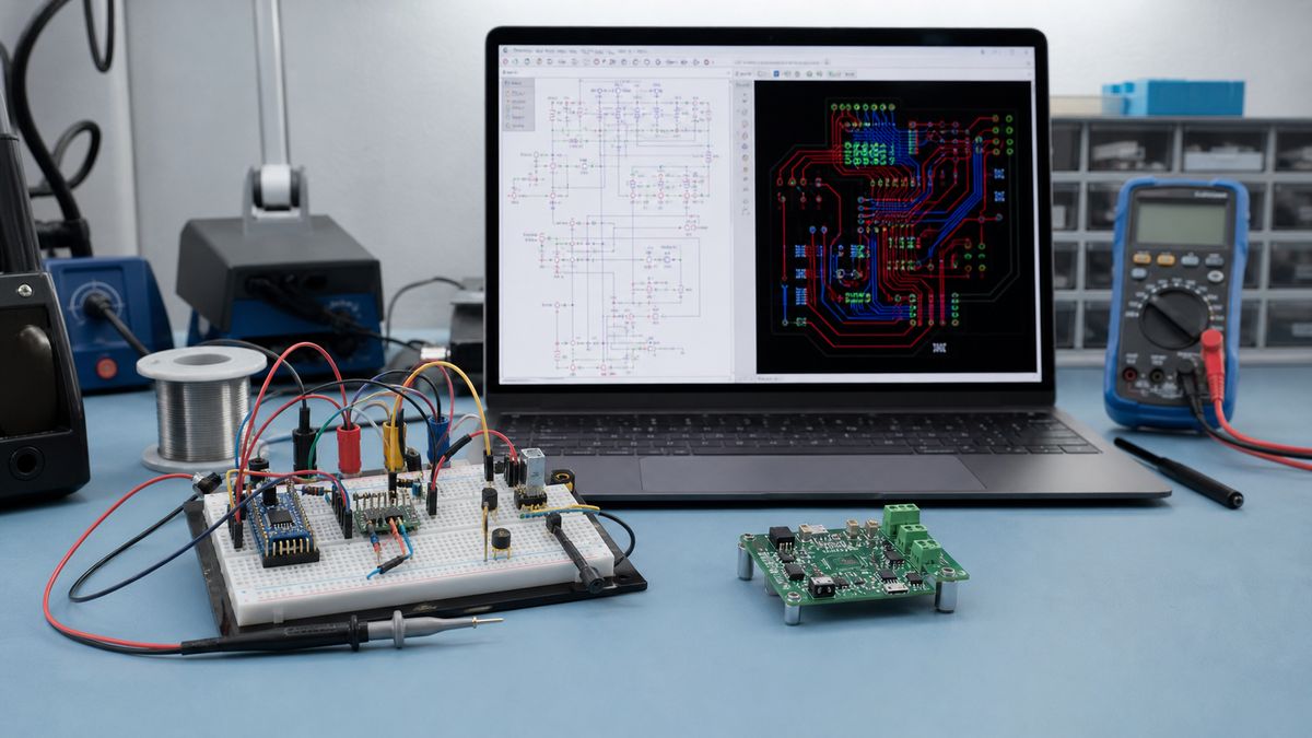
Prove the breadboard actually works
Record supply voltage and current, key waveforms, input/output behavior and operating limits. Test more than one convenient condition. A circuit that works only because of loose wiring, a bench supply limit or accidental capacitance is not a stable design baseline.
Capture every net in a schematic
Photograph the prototype, list every component value and trace each node with power removed. Draw functional blocks first, then connect named nets. Recheck the schematic against the breadboard point by point and use ERC as a prompt for review, not proof of correct behavior.
Replace modules with deliberate circuit choices
A breadboard may use complete regulator, sensor or microcontroller modules. Decide whether the PCB will keep those modules or integrate their circuits. If integrating them, use the original device datasheets and reference designs, including decoupling, boot, reset, programming and protection requirements.
Select exact parts and verify footprints
| Check | Evidence | Failure prevented |
|---|---|---|
| MPN and package | Manufacturer datasheet | Wrong physical part |
| Pin mapping | Symbol-to-footprint audit | Swapped pins |
| Pitch and body | Dimensions and 1:1 print | Part will not fit |
| Polarity/orientation | Assembly drawing and silkscreen | Reverse installation |
| Availability | Approved BOM sources | Unbuildable design |
Add mechanical requirements before placement
Define board outline, mounting holes, connector locations, enclosure clearances, component height, cable direction, controls and keep-outs. Lock these constraints before arranging small parts. A circuit can be electrically correct and still fail because the USB connector misses the opening.
Translate breadboard power into PCB power distribution
Size traces, planes, connectors and protection for real current and voltage. Put decoupling close to the relevant power pins, preserve continuous return paths and separate noisy power stages from sensitive analog nodes. Measure startup and worst-case load, not only idle current.
Place by functional signal flow
Place fixed mechanical items first, then power entry and protection, regulators, processing, interfaces and loads. Keep related parts together. Place crystals and decoupling at their device pins, keep switch nodes compact and leave access for test and programming.
Route with real fabrication rules
Load trace, clearance, via, annular-ring and solder-mask constraints from the intended fabricator. Route critical power and signal paths first, then ordinary connections. Two layers may be enough for a simple board, but do not sacrifice return continuity merely to avoid a justified layer increase.
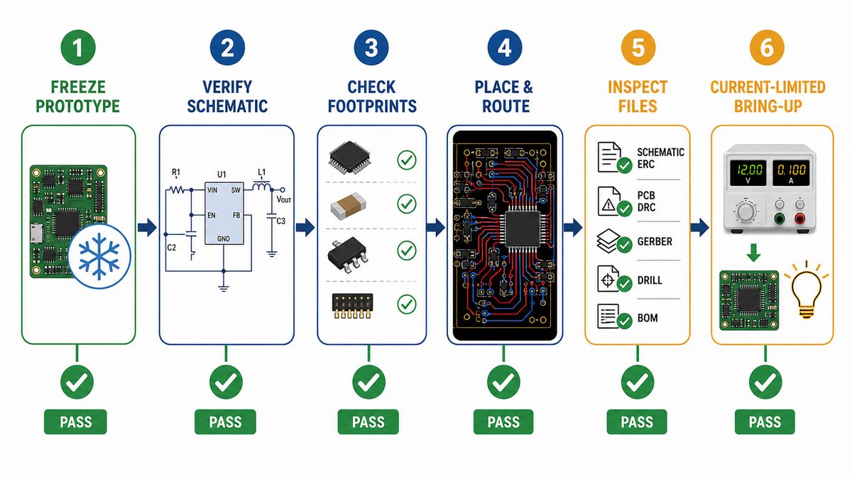
Add testability before the board is crowded
Provide labeled ground, input supply, major rails, reset, programming and important signal test points. Make them accessible to the intended probe or fixture. Write expected readings on the schematic or test plan so bring-up is measurement-driven.
Run checks that software cannot infer
- ERC and DRC items resolved or documented
- Every pin map checked against the datasheet
- Connector mating direction and cable clearance confirmed
- Return paths reviewed across layer changes
- Thermal and current paths checked at worst case
- Polarity and pin-1 markings visible after assembly
- Enclosure and 3D fit reviewed
Prepare a complete manufacturing package
| For PCB fabrication | For assembly | For acceptance |
|---|---|---|
| Gerber or ODB++, drill, outline, stackup, drawing | BOM with MPNs, centroid/CPL, assembly drawings | Test plan, expected readings, visual criteria |
| Material, thickness, copper, finish and quantity | Polarity, substitutions and special process notes | Programming files and revision identity |
Inspect Gerber and drill data in an independent viewer before sending them.
Bring up the first PCB in a controlled order
- Inspect component values, orientation and solder joints.
- Measure resistance from each power rail to ground.
- Apply power with a suitable current limit.
- Verify input protection and each regulator output.
- Check reset, clock and programming access.
- Test one functional block at a time.
- Compare every result with the breadboard baseline and record differences.
Understand why the PCB may behave differently
A breadboard adds long loops, contact resistance, stray capacitance and inductance; a PCB changes those parasitics and return paths. A faster edge, oscillator, analog input or switching regulator may expose issues that were hidden in the prototype. Treat the first board as a controlled experiment, not a guaranteed copy.
Breadboard to PCB FAQ
Can software convert a breadboard photo directly to a PCB?
Automation may assist, but you still need a verified schematic, exact parts, constraints and engineering review. A photograph does not capture electrical intent reliably.
Should I use perfboard before a custom PCB?
Perfboard can provide a useful intermediate prototype when the circuit is simple and changes are still likely. It does not replace final PCB layout validation.
Which PCB software should I use?
Choose a tool that supports schematic capture, footprint verification, layout, ERC/DRC and standard manufacturing outputs.
Can I copy the breadboard component positions?
Usually no. PCB placement should follow mechanics, power, return paths, signal integrity, assembly and test access.
Do I need a two-layer PCB?
Many simple circuits fit two layers, but the correct layer count follows routing density, references, EMC and power needs.
What files does a PCB manufacturer need?
Commonly Gerber or ODB++, drill files and fabrication specifications; add BOM, centroid and drawings for assembly.
Why include test points?
They make rails, programming and important signals accessible without risky probing on fine component pins.
How many prototypes should I order?
Order enough for assembly trials, debugging and destructive investigation while limiting exposure to a possible design revision.
What should I verify before first power?
Inspect orientation and joints, confirm the supply configuration and measure rail-to-ground resistance before using current-limited power.
Review the design before ordering
Send the schematic, layout, fabrication package, BOM and constraints through the PCBTRY contact page for DFM and quotation review before committing the breadboard conversion to production.



1 Comment
When to Use an Evaluation Board vs Custom PCB Design: A Stage-Gate Guide - thindry pcb manufacturer · 08/26/2026 at 08:36
[…] For related next steps, review PCBtry’s guides to custom PCB files and quote checks, moving a prototype into PCB design, and circuit-card assembly test […]