




How do you make a PCB hot-swappable?
For a mechanical keyboard, make the PCB hot-swappable by selecting a specific switch and socket system, using the socket manufacturer’s verified footprint, providing mechanical support and clearance, routing the key matrix and protection circuitry, and defining assembly and full-key testing. Converting an existing soldered PCB with pin sockets is possible only when its holes, plating, clearances and switch system are compatible.
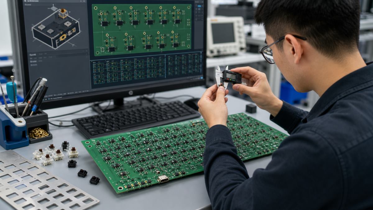
Choose the switch family and socket first
Define the exact switch style, three- or five-pin mechanical support, socket manufacturer and approved part number. Similar-looking sockets are not automatically footprint-compatible. Obtain the current mechanical drawing and land pattern before PCB layout.
Decide between purpose-built sockets and conversion pins
| Approach | Best use | Advantage | Main risk |
|---|---|---|---|
| Surface-mount hot-swap socket | New PCB design and production | Purpose-built replacement workflow | Pad strength, orientation and insertion support |
| Pin-style socket conversion | Compatible plated through-hole PCB | Can preserve an existing design | Hole tolerance and contact fit vary |
| Handwired/printed holder | Experimental one-off builds | Flexible prototype construction | Repeatability and mechanical reliability |
| Standard soldered switch | Lowest-complexity fixed build | Simple joint and footprint | Switch replacement requires desoldering |
Build the footprint from controlled dimensions
Place electrical pads, center opening, locating holes and courtyard from the socket and switch drawings. Add polarity/orientation markings that remain visible during assembly. Validate the footprint with a physical sample before releasing a full keyboard panel.
Provide support for switch insertion force
A hot-swap socket can lift from its pads if a bent switch pin or unsupported PCB receives excessive force. Coordinate the PCB, plate, foam and case so the board is supported without bending. Assembly instructions should require straight pins and controlled insertion.
Check socket clearance on both PCB sides
Review neighboring sockets, diodes, LEDs, stabilizer hardware, fasteners, battery space and enclosure features in 3D and with drawings. Ensure the socket opening remains accessible and that a bottom case rib cannot press on solder joints.
Design the key matrix and diode orientation
Assign rows and columns consistently and place a diode for each key when the matrix architecture requires it. Keep schematic symbols, footprints, silkscreen polarity and placement rotations aligned. Document unused layout options so assembly does not populate conflicting positions.
Protect USB and controller interfaces
Use the connector, ESD protection, power filtering and controller reference requirements appropriate to the design. Mechanical reinforcement and daughterboard cables may reduce connector stress. Do not let the hot-swap feature distract from basic USB, power and firmware reliability.
Plan optional layouts without creating collisions
Multiple switch positions can support ANSI/ISO or split keys, but overlapping sockets, stabilizers and traces can make a layout impossible to assemble. Build a configuration matrix and check every supported combination. Remove untested combinations from public claims.
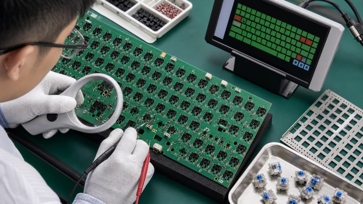
Make the socket pads resistant to handling damage
Use the approved land pattern, mask definition and copper connection strategy, then review pad stress with the fabricator and assembler. Do not enlarge or anchor pads arbitrarily if it violates spacing or soldering behavior. Socket retention depends on PCB construction, solder process and product support together.
Prepare the assembly package
Supply Gerber/ODB++, BOM with exact socket and switch-related parts, CPL, assembly drawings, polarity notes, approved layout options and first-article criteria. If sockets are hand-placed or fixture-dependent, state the support and inspection method.
Control solder paste and reflow for sockets
Review paste apertures, board support, placement pressure and reflow profile using the socket supplier and solder-process guidance. A socket can appear present while one pad is poorly wetted. First-article inspection should cover orientation, coplanarity and both solder joints.
Test the bare PCBA before installing switches
Confirm USB detection and firmware, then test every key position with an approved conductive fixture or test method. Record results by matrix coordinate or layout position. A whole failed row/column suggests a shared path, while one failed key points toward its local socket, diode or trace.
| Failure pattern | Likely area | Next check |
|---|---|---|
| One key never registers | Socket, diode, pad or local trace | Inspect and compare with adjacent working key |
| Entire row/column fails | Shared matrix path or controller pin | Trace continuity and firmware assignment |
| Key works only with pressure | Socket contact or solder joint | Inspect fit and socket attachment |
| Wrong key reports | Matrix mapping or bridge | Check schematic/firmware and nearby joints |
| Socket lifts during insertion | Bent pin, poor solder or weak support | Stop insertion and repair before pad damage spreads |
Validate repeated switch replacement
Use representative switches and the final plate/case support to run a defined insertion/removal evaluation when product requirements demand it. Inspect socket retention, contact behavior, pads and PCB deflection afterward. Do not publish an insertion-cycle claim without traceable test evidence.
Know the limits of converting a soldered PCB
Pin sockets require compatible finished holes and plated barrels; large surface-mount sockets require their own land pattern and cannot simply be added to an unrelated board. Drilling or scraping a finished PCB can destroy traces and plating. Treat conversion as a separately verified repair/modification project.
Hot-swap PCB release checklist
- Exact socket and switch system are named.
- Footprint matches controlled drawings and a physical sample.
- Plate, case and PCB support insertion force.
- Socket, diode, stabilizer and enclosure clearances pass.
- Matrix and polarity agree across schematic and placement data.
- Assembly process controls both socket joints.
- Every key position passes bare-PCBA testing.
- Repeated insertion claims have defined evidence.
Hot-swappable PCB FAQ
Can any keyboard PCB be made hot-swappable?
No. Conversion depends on hole dimensions, plating, footprint space, switch system and mechanical support.
Are all hot-swap sockets interchangeable?
No. Use the exact manufacturer’s mechanical drawing, land pattern and approved switch compatibility.
Do hot-swap sockets eliminate soldering?
They eliminate soldering each replaceable switch, but the sockets and other PCBA parts still require assembly.
Why do sockets lift off the PCB?
Common contributors include bent switch pins, unsupported insertion, damaged pads or poor solder joints.
Can five-pin switches fit a three-pin PCB?
Only after product-specific compatibility checks; cutting locating pins changes switch support and should not be assumed acceptable.
How is every key tested before assembly?
Use an approved fixture or bridge method with the correct firmware and record every matrix position.
Does a plate matter on a hot-swap keyboard?
Yes. It helps align and support switches and affects force transferred to the sockets and PCB.
What files are needed for manufacturing?
Provide PCB data, BOM, CPL, assembly drawings, firmware/test method, layout matrix and acceptance criteria.
Request hot-swap keyboard PCB review
Send the schematic, PCB files, exact socket and switch MPNs, mechanical stack, firmware and key-test plan through the PCBTRY contact page. Review the footprint and support structure before prototype fabrication.



1 Comment
Hot-Swap PCB vs Soldered PCB: Differences, Pros, Cons and Which to Choose - thindry pcb manufacturer · 08/20/2026 at 09:01
[…] That distinction explains both the convenience and the design responsibility. Hot-swap removes soldering from the routine switch-change operation, but it does not remove solder-joint design, land-pattern accuracy, component placement, inspection, or mechanical support from manufacturing. For the implementation details, see PCBtry’s guide to making a PCB hot-swappable. […]