




How do you make a PCB stencil?
Create the stencil from the PCB solder-paste layer, not from the copper or solder-mask layer. Verify revision and scale, review aperture dimensions and stencil thickness with the assembly process, add useful board alignment features, then laser-cut or order the stencil in a suitable material. The stencil is accepted only after a first print shows repeatable paste deposits without bridging, skips or poor release.
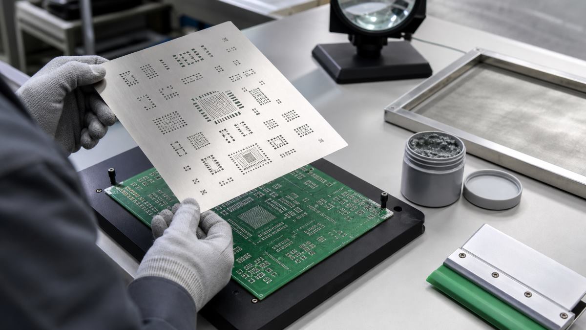
Decide whether to make or order the stencil
DIY polymer stencils can work for coarse prototype boards and low quantities. Laser-cut stainless steel is usually more repeatable for fine pitch, small apertures, production volumes or process validation. Choose from package risk and print consistency, not only purchase price.
Freeze the PCB revision before exporting data
The paste layer, component footprints, BOM and placement data must describe the same board revision. Remove unused variants and confirm which side or sides require printing. A perfect stencil for the wrong revision can deposit paste onto missing or shifted pads.
Export the top and bottom paste layers
Generate Gerber paste data or the stencil supplier’s requested format directly from the PCB CAD tool. Include a clear board outline or registration reference without turning unrelated mechanical graphics into apertures. View the export at 1:1 scale and check both sides separately.
Review every aperture class
Group apertures by package: fine-pitch leads, bottom-terminated pads, small passives, large thermal pads and through-hole paste features if used. Footprint paste openings are a starting point, not an automatic final answer. Assembly process engineering should approve reductions, windowing and special shapes.
| Feature | Print risk | Review question |
|---|---|---|
| Fine-pitch leads | Bridging or poor release | Do aperture width and stencil thickness support reliable release? |
| Small passives | Unequal deposits and tombstoning | Are paired apertures balanced? |
| Thermal pads | Excess paste and voiding | Should the opening be divided into windows? |
| Large connectors | Insufficient solder or board movement | Does the joint need a process-specific aperture? |
| Mixed package sizes | One thickness cannot satisfy all deposits | Is a stepped stencil or process split justified? |
Select stencil thickness with the smallest apertures in mind
Thickness affects deposited paste volume and aperture release. A thicker sheet is not automatically better for large joints because it can make fine apertures difficult to release. Use the assembler’s process capability, paste type and package geometry to set the thickness.
Choose framed or frameless construction
Framed stencils support repeatable printer tension and higher-volume use. Frameless prototype stencils reduce cost and storage but require a stable holder or jig. Specify usable stencil area, board position, squeegee direction and any frame system before manufacture.
Add alignment and handling features
Provide enough stencil margin for taping, clamping or the printer frame. Fiducials can support automated alignment when the process uses them. A simple prototype jig can use spare PCBs of equal thickness around the target board so the stencil lies flat and cannot slide.
Use a safe, controlled cutting method
Laser, chemical and mechanical cutting processes depend on the material and equipment. Do not cut unknown polymers: fumes, fire behavior and machine compatibility must be verified. DIY methods should never be used where aperture accuracy, burr control or material safety cannot be demonstrated.
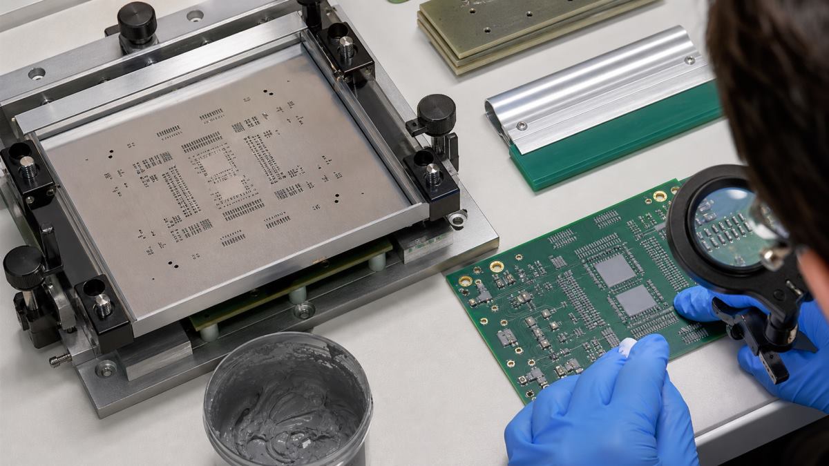
Inspect the finished stencil before printing
Check revision, side, scale, orientation, aperture completeness, blocked openings, burrs and damage. Confirm the board outline and registration marks align with the physical PCB. Protect sharp metal edges and store the stencil flat or in its intended frame.
Prepare the PCB and solder paste
Use clean, dry boards and solder paste stored, conditioned and mixed according to its current supplier instructions. Identify the paste lot and working time. Do not compensate for old or poorly handled paste by changing stencil pressure.
Align the stencil without smearing deposits
Fix the PCB in a repeatable nest, lower the stencil so apertures center on pads, and clamp or tape the setup. The stencil should contact the board evenly. Lift it vertically after printing; sideways movement can smear neighboring deposits.
Make one controlled squeegee pass
Use a suitable squeegee angle, pressure and speed to roll paste across the apertures and leave the stencil surface reasonably clean. Multiple random passes can change deposit volume. Record the settings that produce an acceptable first print.
Inspect the first paste print
| Observation | Likely cause | Next action |
|---|---|---|
| Bridges between pads | Misalignment, excessive deposit or smear | Clean, realign and review aperture/process |
| Incomplete deposit | Blocked aperture or poor release | Clean underside and review aperture/thickness |
| Offset deposits | Board or stencil movement | Improve fixture and alignment |
| Paste left in apertures | Release problem or paste condition | Check cleaning, paste and area ratio with supplier |
| Unequal paired pads | Stencil damage or aperture imbalance | Inspect stencil and footprint paste design |
Clean and store the stencil correctly
Use a cleaning method compatible with the paste and stencil material, and keep residue from drying in fine apertures. Inspect both sides after cleaning. Store the stencil protected from bending, scratches and contamination, with revision identification attached.
Use this PCB stencil release checklist
- Paste data matches the released PCB revision.
- Top and bottom stencils are clearly identified.
- Aperture changes have an engineering reason.
- Thickness matches package mix and printing process.
- Frame, margin, fiducials and board position are defined.
- Stencil passes scale, burr and aperture inspection.
- First print is aligned, complete and repeatable.
- Cleaning, storage and revision controls are documented.
PCB stencil FAQ
Can I use the solder-mask Gerber to make a stencil?
No. Use the solder-paste layer; mask openings serve a different purpose and often have different dimensions.
Can a craft cutter make a stencil?
It can suit some coarse prototypes if material and accuracy are validated, but it may not resolve fine-pitch apertures reliably.
Is stainless steel always necessary?
No, but it is generally preferred when repeatability, fine features, durability or production control matters.
Should apertures equal copper-pad size?
Not automatically. Paste apertures may need process-specific reductions, shapes or windowing.
Why does paste stay in the stencil?
Possible causes include aperture geometry, stencil thickness, contamination, paste condition and lift technique.
Do I need separate stencils for both PCB sides?
Double-sided SMT assembly normally uses distinct paste patterns for each side unless the process is intentionally different.
How do I align a frameless prototype stencil?
Use a flat board nest or same-thickness surrounding boards, fixed stops and clear registration references.
What should I send with a stencil order?
Send paste Gerbers, board outline, revision, side, thickness/process request, frame format and special aperture notes.
Request PCB and stencil engineering review
Send the PCB fabrication files, paste layers, BOM, placement data, package risks and assembly quantity through the PCBTRY contact page. The PCB and stencil should be reviewed together before the first assembly build.



0 Comments