




The Short Answer: Use Each Board for Different Evidence
Use an evaluation board when the main uncertainty is whether a device, interface, algorithm, or firmware stack can perform the required function. Start a custom PCB when the remaining questions depend on your product’s actual power tree, connectors, mechanics, thermal path, antenna environment, test strategy, bill of materials, or production controls. If the processor or radio is difficult to design around but the product needs custom I/O and mechanics, a qualified module on a custom carrier can be the lower-risk middle path.
The decision is not “prototype versus professional hardware.” It is an evidence decision. Keep the evaluation board only while it can produce the evidence needed for the next business and engineering decision. Move when the unanswered risks are created by the final board and cannot be resolved on the vendor platform.
| Choose this path | Advantages | Limitations | Use it when |
|---|---|---|---|
| Evaluation board/EVM/EVK | Fast access to silicon, debug features and a documented known-good platform | Bench-oriented mechanics and circuitry do not represent final-product conditions | Silicon selection, firmware learning, interface experiments and bench measurements remain the main work |
| Module plus carrier PCB | Retains a complex compute or radio subsystem while allowing custom I/O, protection and mechanics | Module cost, availability, constraints and supplier dependence remain | The module covers the highest-risk function and a carrier can satisfy the remaining product requirements |
| Fully custom PCB | Maximum control over size, power, interfaces, BOM, test access and lifecycle | Highest design, validation, bring-up and sustaining responsibility | Board-level requirements and project economics justify full hardware ownership |
What an Evaluation Board Proves—and What It Does Not
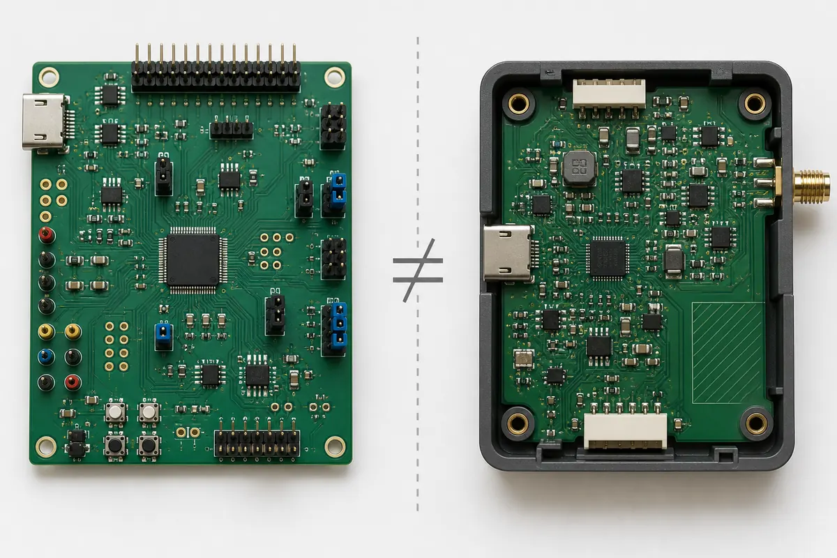
An evaluation board is a controlled platform designed to make a component accessible. It may provide a known power supply, recommended decoupling, test points, configuration jumpers, connectors and a documented layout. That makes it valuable for comparing devices, learning software, confirming basic peripheral operation and reproducing a question with the semiconductor vendor.
Analog Devices notes that evaluation boards let engineers evaluate an IC without first constructing a prototype, while also warning that blindly inserting an evaluation-board layout into a larger system may not be appropriate. The board is a small system with its own grounding, parasitics and operating context. Texas Instruments EVM guides likewise commonly provide schematics, layouts and bills of materials as engineering references; those documents must be read with the device data sheet and layout requirements.
| Evidence from an evaluation board | What remains unproven |
|---|---|
| The device boots and required firmware features can run | Your final clocking, reset, boot, memory and programming implementation |
| An interface works with bench wiring or supplied peripherals | Signal integrity, protection and connector behavior on the product PCB |
| Typical power modes can be measured | Battery life and rail margin with the final regulator, loads and duty cycle |
| RF communication works on the vendor platform | Antenna performance in the final enclosure beside batteries, cables and displays |
| The IC operates thermally on the EVM | Junction temperature in the final copper area, airflow and enclosure |
| Firmware is functionally promising | Product EMC, safety, environmental and regulatory results |
Keep a written “proven / not yet proven” list. It prevents a successful demonstration from silently becoming an unsupported qualification claim.
Three Practical Paths: EVM, Module Plus Carrier, or Custom PCB
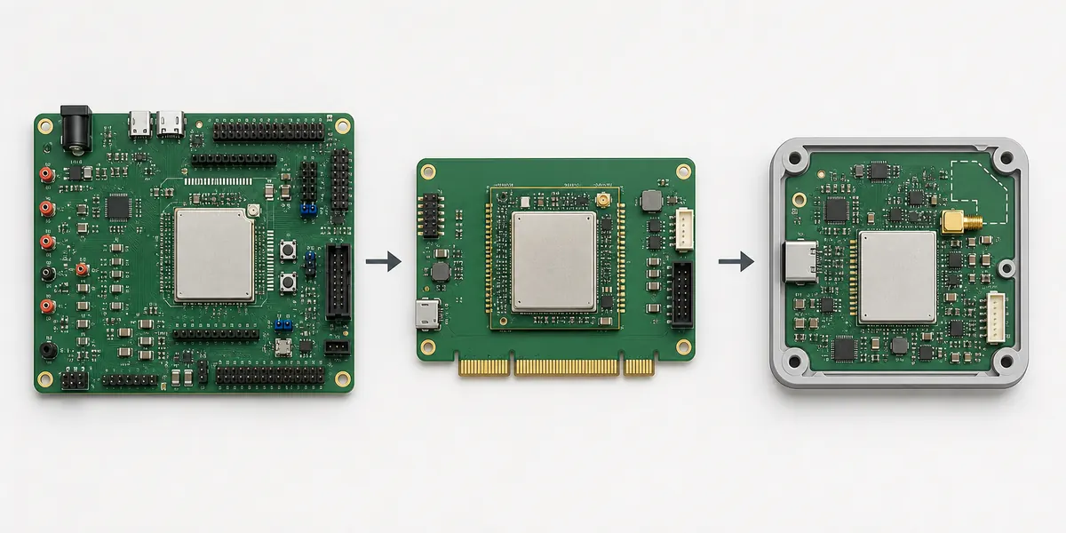
Continue with the evaluation board when requirements are still moving, pin usage is unsettled, or the team is comparing silicon. The board is especially useful as a known-good reference during firmware development and later fault isolation.
Choose a module plus carrier when a module already solves a high-risk function—such as an RF subsystem or complex processor—and the product mainly needs tailored power, connectors, protection, sensors and mechanical integration. Confirm module lifecycle, documentation, antenna conditions, certifications and production programming; a carrier board still requires engineering and validation.
Choose a fully custom PCB when the architecture is stable enough to own. Typical reasons include a constrained enclosure, unusual interfaces, lower power, controlled impedance, defined thermal spreading, production test access, security provisions, lifecycle control or a project-specific cost case. Custom design transfers responsibility to your team for schematic correctness, layout, component substitutions, bring-up, compliance evidence and sustaining engineering.
Decision Matrix: When to Stay and When to Move
| Requirement | Stay on the EVM when | Move toward custom hardware when | Evidence required |
|---|---|---|---|
| Core function | Device selection or firmware feasibility is unresolved | Functions and essential pins are defined | Requirements-to-test traceability |
| Power | You are comparing modes and estimating loads | Rail sequencing, peak current, battery and efficiency affect the product | Power budget and measured load profiles |
| Mechanics | Enclosure and connectors remain fluid | Outline, mounting, keep-outs and connector positions are controlled | Mechanical drawing and 3D clearance review |
| RF/EMC | You are validating protocol and software | Antenna placement, cables, switching supplies or emissions depend on layout | RF plan, stackup constraints and pre-compliance plan |
| Production | Only bench quantities are needed | Programming, test, traceability and assembly yield matter | Test coverage and manufacturing requirements |
| Lifecycle | Short experiments tolerate board changes | The product needs controlled components and revisions | Approved parts and lifecycle ownership |
Do not freeze a custom schematic merely because firmware ran once. Freeze when the requirements that determine schematic and layout choices are sufficiently stable and unresolved items have named owners.
Electrical, Thermal and RF Limits That Trigger Custom Hardware
Custom hardware becomes necessary when the variable being tested is the product board itself. A regulator evaluated at a convenient bench load does not establish performance with your transient profile, copper resistance and thermal environment. A fast interface proven over short EVM traces does not establish margin through your connector, layer stack and routing. An RF link demonstrated in open air does not establish antenna efficiency inside a compact enclosure.
Before schematic capture, document maximum and typical loads, rail tolerance, sequencing, inrush, sleep current, fault protection and measurement conditions. For thermal work, identify dissipating components, heat paths, ambient assumptions and temperature limits. For RF, document antenna type, keep-out, enclosure materials, cable placement and required regional variants. These inputs guide layout and later validation; they are not proof of final performance.
Mechanics, EMC and Certification Change the Decision
An EVM usually prioritizes access over product packaging. Headers, debug interfaces and generous spacing may be useful on a bench but incompatible with the enclosure. A custom PCB lets the team control mounting, connector orientation, board-to-board interfaces, shielding and cable exits. Those choices can also change emissions, immunity and electrostatic-discharge behavior.
Certification requirements belong in the architecture discussion before layout. Determine applicable markets and standards with qualified compliance specialists. Existing module approvals may reduce some work only under their stated conditions; they do not automatically certify the finished product. Preserve design records, component versions, firmware versions and test configurations so results are traceable.
BOM, Supply Chain and Unit Economics Without a Fake Break-Even
There is no universal production quantity at which a custom PCB becomes cheaper. Use a project-specific model:
Total custom cost = design and review effort + prototypes and re-spins + fixtures and programming + compliance work + quantity × landed unit cost + sustaining cost.
Compare that with the purchased-board or module cost, carrier cost, integration labor, cables, enclosure impact, supply risk and expected quantity. Also consider minimum orders, lead time, alternates, licensing, lifecycle notices and the cost of maintaining firmware for board revisions. Record assumptions and calculate several quantity and redesign scenarios. A custom board can improve unit economics and control, but only if the avoided integration cost exceeds the additional engineering and ownership burden.
How to Run Firmware and Custom PCB Work in Parallel
The EVM does not become useless when custom design starts. Keep it as a known-good platform while the hardware team captures the schematic and layout. Firmware can develop algorithms, drivers and automated tests on the EVM, provided hardware dependencies are tracked.
| Continue on the EVM | Prepare for the custom board |
|---|---|
| Driver and protocol development | Pin mapping and peripheral-instance verification |
| Functional test automation | Programming, recovery and factory-test interfaces |
| Reference measurements | Expected rails, clocks and bring-up checkpoints |
| Reproduction of vendor support questions | Board abstraction and revision control |
When first boards arrive, begin with controlled current limits and a written bring-up sequence. Compare measurements with both design expectations and the known-good EVM. Differences are diagnostic evidence, not automatic proof that either platform is wrong.
A Stage-Gate Plan for the First Custom PCB Spin
Download the Evaluation Board vs Custom PCB Decision Worksheet (PDF). This original worksheet is based on the manufacturer sources listed in the document. It is a blank planning aid, not a customer record, test report, certification decision or engineering approval.
- Gate 1—silicon evidence: confirm essential functions, toolchain and vendor support. Exit with a device decision and unresolved-risk list.
- Gate 2—requirements: freeze essential interfaces, power modes, mechanics, environment, markets and production assumptions. Exit with owned requirements.
- Gate 3—architecture: choose EVM, module/carrier or custom implementation. Exit with documented tradeoffs and lifecycle ownership.
- Gate 4—design review: review schematic, stackup, placement constraints, protection, test access and manufacturing data. Exit only when issues have owners.
- Gate 5—prototype and bring-up: inspect assembly, power rails, clocks, reset and programming before full functional tests.
- Gate 6—product validation: test the actual board in representative mechanical, thermal, electrical and firmware conditions; plan appropriate compliance work.
- Gate 7—production handoff: release controlled files, approved parts, programming instructions, inspection criteria and test coverage.
Common Transition Mistakes
Published engineering scenario: I2C worked on the evaluation board but failed on the custom board
This is a public Analog Devices EngineerZone support scenario, not a PCBtry customer case. An engineer reported that ADAU1966A I2C read and write operations worked on the evaluation board but returned incorrect values on a custom board. Oscilloscope decoding showed that commands were being issued, and using the evaluation-board programmer did not remove the problem.
The investigation first considered pull-up resistance and logic-low voltage. The engineer changed the pull-up resistors but the fault remained. The decisive finding was that the custom board supplied 5 V to an input whose maximum was 3.3 V. Correcting the supply to 3.3 V restored I2C operation. The result is reported by the original poster in the verified-answer thread: I2C configuration works with evaluation board, but not with custom board.
The lesson is narrow but useful: firmware and commands validated on an EVM do not prove that a custom board has reproduced the required electrical conditions. During bring-up, compare supply domains, absolute limits, pull-ups, reset, clocks and interface waveforms against both the data sheet and the known-good platform. Do not jump directly to a software explanation merely because the same software worked on the EVM.
- Copying a reference layout without context: reuse guidance only after checking stackup, return paths, placement, interfaces and vendor notes.
- Freezing before requirements stabilize: unresolved connectors, power modes or mechanics create expensive layout changes.
- Removing debug access too early: preserve practical programming, recovery and measurement points.
- Using a universal cost threshold: calculate with your NRE, quantity, test and compliance assumptions.
- Testing only functionality: add margins, faults, temperature, enclosure and production variation appropriate to the product.
- Abandoning the EVM: retain it as a reference for firmware and fault isolation.
Evaluation Board vs Custom PCB FAQs
Is an evaluation board the same as a development board?
The terms overlap, but an evaluation board often focuses on evaluating a specific device, while a development board may provide a broader software and prototyping ecosystem. Read the manufacturer’s intended-use documentation.
Can an evaluation board be used in a finished product?
Do not assume so. Check intended use, license, lifecycle, environmental ratings, certifications, connectors, mechanical security and production support for the exact board and product.
When should firmware development leave the evaluation board?
Keep platform-independent work on the EVM while custom hardware is developed, then move hardware-dependent validation to the custom PCB as soon as stable prototypes are available.
Does a working EVM prove the custom PCB will work?
No. It reduces device and firmware uncertainty, but the custom board introduces its own power, layout, signal-integrity, thermal, mechanical and assembly conditions.
Should I copy the evaluation-board schematic and layout?
Use them as references only within vendor documentation and licensing. Confirm every circuit, component and layout choice against your requirements, data sheets and design guides.
Is a module and carrier better than a fully custom PCB?
It can reduce compute or RF design risk while allowing custom I/O and mechanics. The tradeoff is module cost, availability, constraints and continued supplier dependence.
At what volume does a custom PCB become worthwhile?
There is no universal volume. Compare NRE, prototypes, fixtures, compliance, landed unit cost, integration labor, lifecycle risk and sustaining effort using your forecast.
What must be stable before starting a custom PCB?
At minimum, essential functions, pin use, power modes, mechanical constraints, interfaces, target environment and validation ownership should be sufficiently defined.
What should the first custom PCB prototype test?
Start with assembly condition, shorts, rail sequencing, current, clocks, reset and programming; then expand to interfaces, performance, faults and representative product conditions.
Should the evaluation board be kept after custom hardware works?
Yes. A known-good vendor platform can remain useful for software comparison, component evaluation and vendor-support reproduction.
Prepare a Better Custom PCB RFQ
Once the stage-gate decision supports custom hardware, prepare controlled fabrication and assembly inputs: schematic and PCB files, Gerbers or ODB++ as applicable, drill data, stackup and impedance requirements, board outline, material and finish, BOM with manufacturer part numbers, placement data, drawings, quantity, inspection expectations and test requirements. For related next steps, review PCBtry’s guides to custom PCB files and quote checks, moving a prototype into PCB design, and circuit-card assembly test coverage.
PCBtry can review fabrication and assembly information for manufacturability and quotation. Product architecture, regulatory scope and final validation acceptance remain the responsibility of the appropriately qualified product team.



0 Comments