




The Short Answer: Choose the Circuit-Formation Method Before Freezing Geometry
Subtractive etching and semi-additive patterning solve the same basic problem—forming copper conductors—but they create different DFM constraints. In a conventional subtractive flow, the fabricator starts with copper-clad material and removes unwanted copper. In a semi-additive flow, a very thin base layer or seed layer is used, copper is built where the circuit requires it, and residual base copper is removed in a final controlled step. That difference changes what must be confirmed before a dense layout is released.
Use subtractive processing when the required geometry, copper distribution and tolerance can be supported by the approved fabricator’s conventional capability. Start a SAP or mSAP discussion when the design depends on fine features or trace-profile control that cannot be assumed from a conventional etch rule. Do not choose by a generic “minimum line/space” table: the answer depends on layer type, copper thickness, material, panel format, imaging, plating, registration, inspection method and production evidence.
| Decision question | What to obtain before release |
|---|---|
| Can conventional etching support the feature? | Fabricator-specific DFM rule and the copper condition to which it applies |
| Is semi-additive processing justified? | Named geometry or performance risk plus approved process capability evidence |
| Can the design move to quotation? | Stackup, layer build, inspection, coupon and CAM-review requirements |
How Subtractive Etching and Semi-Additive Patterning Form Copper
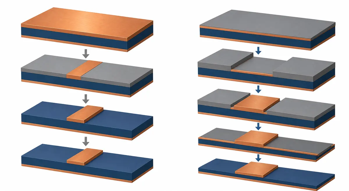
In a conventional subtractive circuit-formation flow, a copper-clad surface is imaged, protected where conductors are wanted, and etched where copper is unwanted. Because the etchant removes copper from exposed areas while also acting laterally, the final conductor profile can differ from the resist image. The relationship between copper thickness, feature width, etch chemistry and compensation is a practical DFM issue; see PCBtry’s guide to etch factor, undercut and CAM compensation for the related conventional-etch context.
SAP and mSAP descriptions vary between suppliers, but the common principle is selective copper build-up on a thin conductive base. A resist pattern defines where copper is plated; after resist removal, a controlled flash etch removes exposed base copper while retaining the plated conductors. Altium’s SAP overview and Mitsui Kinzoku’s circuit-formation comparison describe this distinction. The precise sequence, starting copper and supported geometry remain process-specific.
Why Starting Copper Changes Undercut, Trace Profile and DFM Margin
A thicker copper layer normally requires more copper removal in a subtractive flow. That raises the importance of lateral etching and shape compensation. A semi-additive process begins with far less base copper and builds the conductor selectively, so the final flash-etch task is different. The potential benefit is not a magic line-space number; it is a different balance of imaging, plating and residual-copper-removal controls.
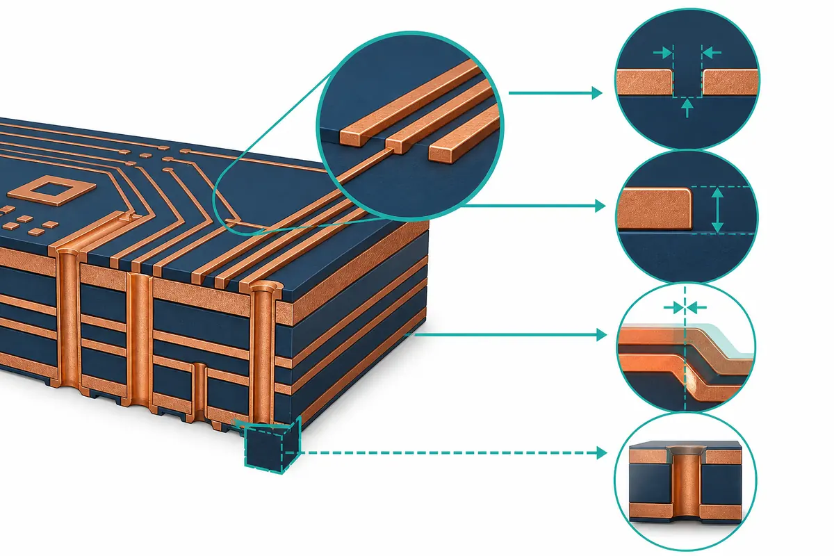
For a controlled-impedance or high-density design, ask how the fabricator defines finished conductor width and thickness, what cross-section evidence is available, and what tolerance applies to the requested material and layer. A nominal CAD width is not proof of finished geometry. If a design decision depends on profile, request an appropriate coupon, microsection plan or other agreed inspection evidence.
SAP, mSAP and Subtractive: Do Not Treat the Names as a Capability Table
“SAP,” “mSAP,” and related proprietary names are frequently used as if they always identify the same capability. They do not. AT&S describes mSAP as selectively applying conductor material rather than etching traces from a conventional copper layer; GS Swiss PCB notes that achievable geometry is linked to conductor height. Those statements explain the principle, not a blanket acceptance limit for every board.
| Process family | Useful DFM interpretation | Do not assume |
|---|---|---|
| Subtractive | Confirm copper thickness, compensation, profile and etch-rule margin. | That a rule for one copper weight or layer applies to all layers. |
| mSAP | Confirm thin-base-copper flow, imaging, pattern plating, flash etch and inspection. | That every supplier uses the same starting foil or supports the same geometry. |
| SAP | Confirm the seed-layer, activation, plating and final-removal flow for the exact technology. | That a name alone proves package-substrate capability or volume yield. |
DFM Decision Matrix: Geometry, Copper, Imaging, Plating and Inspection
| DFM item | Subtractive emphasis | Semi-additive emphasis | Evidence to request |
|---|---|---|---|
| Line and space | Etch compensation and remaining margin | Imaging, resist opening and plating definition | Approved capability for material, layer and copper condition |
| Finished copper | Starting foil and etch profile | Base layer plus plated build-up and uniformity | Finished-copper target and inspection method |
| Registration | Artwork and layer registration | Registration plus fine-feature imaging alignment | Stackup, datum strategy and tolerances |
| Inspection | Etch quality and conductor geometry | Plating, residual copper removal and fine-feature defects | Coupon, AOI and microsection agreement where applicable |
What to Put in the Fabricator Capability Request
Download the SAP vs Subtractive PCB DFM Questionnaire (PDF). This original planning worksheet is based on the public sources listed in the document. It is not a capability certificate, test report, customer record, approval or substitute for supplier CAM review.
Give the fabricator the design facts, not only a desired process name: intended layer count and stackup, material family, copper targets, critical line/space locations, controlled-impedance requirements, via structure, pad and solder-mask constraints, panel or array constraints, quantity, intended inspection and any reliability requirements. Ask which layers can use which process, what finished geometry is controlled, which conditions limit the rule, and what evidence can support acceptance.
A request that says only “use mSAP” invites ambiguity. A request that identifies the critical nets, geometry, copper condition, inspection need and volume stage gives CAM and process engineering something testable.
Stackup, Vias and Registration: Process Selection Is Not Only Line and Space
Fine routing is one part of a board. Stackup construction, dielectric thickness, via sequence, plating requirements, surface finish, solder-mask registration and test access may become the actual release constraint. For a broader manufacturing-input review, see PCBtry’s guide to multilayer PCB stackup, lamination and DFM checks.
Do not reduce a semi-additive decision to one BGA escape feature. Identify the feature that drives the process, then check whether adjacent pads, vias, reference planes, mask openings, fabrication coupon and inspection approach remain compatible with the approved flow.
A Traceable Fine-Line Patterning Scenario and Its Limits
Mitsui Kinzoku’s published process comparison contrasts a conventional flow that includes hard etching with an mSAP flow using pattern plating followed by flash etching. The engineering lesson is that changing the circuit-formation flow changes the process controls that must be qualified: the hard-etch profile concern is not simply carried over unchanged to the flash-etch step.
This is a published technology comparison, not a PCBtry customer result, production-yield report or guarantee. It does not establish a specific line/space, cost or reliability outcome for another fabricator. The actionable step is to ask the selected supplier how its own process flow, starting copper and inspection plan apply to the requested layer.
How to Validate the Choice on the First Build
Turn the process decision into a controlled first-build plan. Before fabrication, record the exact revision of the stackup, the critical layers, the requested finished copper condition, the location of each process-driving feature and the acceptance method. The fabricator’s CAM response should either confirm each item or identify a revision needed for its qualified flow. “Capability confirmed” without those inputs is not enough to prove that the specific layout can be built as intended.
For the first build, compare the manufactured result with the agreed drawing and fabrication notes rather than only checking whether the board powers up. Where the project and supplier agreement call for it, review the relevant dimensional evidence, coupon or microsection observations, continuity and isolation checks, and any critical impedance or assembly findings. Keep the evidence tied to the exact material, panel, revision and quantity stage. A successful sample can reduce uncertainty, but it should not be silently promoted into a volume-yield or reliability claim.
If a feature is adjusted during CAM, update the design record and evaluate adjacent rules. A trace-width change can affect spacing; a copper or stackup change can affect impedance assumptions; a pad or via adjustment can affect assembly and test access. The goal is not to force one process name onto the design. The goal is to maintain a traceable chain from the product requirement to the approved geometry, chosen circuit-formation flow and verification evidence.
Document exceptions explicitly. If the supplier accepts a feature only on a named layer, material or panel flow, record that condition in the fabrication notes and do not apply the exception to unrelated layers. That record is also useful when later revisions, alternate sources or cost reviews reopen the process decision.
Common SAP vs Subtractive DFM Mistakes
- Copying a supplier’s headline minimum: use the capability conditions, not the marketing headline.
- Calling SAP and mSAP interchangeable: obtain the actual process definition.
- Specifying CAD geometry only: define finished copper, tolerances and inspection evidence.
- Ignoring stackup and vias: assess the complete layer and build sequence.
- Assuming a prototype proves volume readiness: define quantity stage, panel controls and acceptance evidence.
- Using generic etch advice for production fine lines: request supplier CAM review.
Semi-Additive vs Subtractive Etching FAQs
Is SAP the same as mSAP?
No universal equivalence should be assumed. Ask the fabricator for its specific base-copper or seed-layer, plating and residual-copper-removal flow.
Does semi-additive processing eliminate etching?
Not necessarily. Many semi-additive flows include controlled removal of exposed residual copper after pattern plating.
Does SAP always make a PCB cheaper?
No. Process cost, yield, layer count, material, geometry and volume all require a project-specific model.
What is the first DFM question for fine traces?
Ask for the approved finished geometry and its exact material, copper, layer and inspection conditions.
Can a subtractive layer and a semi-additive layer coexist?
That is process- and fabricator-specific. Confirm the layer assignment and build sequence during CAM review.
Does a smaller line/space automatically improve impedance?
No. Impedance depends on the complete geometry, dielectric, reference plane and finished-conductor profile.
What inspection is relevant?
Agree on suitable geometry, plating, residual-copper and defect inspection evidence for the critical features.
Do I need a special stackup?
Possibly. The selected process may affect copper, dielectric, registration and via assumptions; use an approved stackup.
Can an etch-factor rule prove SAP capability?
No. It helps explain subtractive etch behavior, but it is not a SAP capability qualification.
When should the fabricator review the design?
Before geometry and stackup are frozen, especially when a feature drives process selection.
Prepare a Fabrication Package for CAM Review
Provide controlled PCB data, layer stackup, drill and via information, impedance requirements, material and copper assumptions, critical-net locations, drawings, fabrication notes, quantity and acceptance expectations. PCBtry can review fabrication and assembly information for manufacturability and quotation; the product team remains responsible for architecture, qualification and final acceptance.



0 Comments