




Start with the Product Boundary, Not an Antenna Trace
A useful 433 MHz PCB antenna layout starts with the product that will surround the antenna. The radio frequency is only one input. Before drawing copper, record the intended sales region, radio IC and output network, board outline, layer stack, available board edge, ground-plane extent, enclosure material, battery position, cables, displays, fasteners and the ways a user may hold or mount the product. These items can change the impedance and radiation behavior of the assembled device.
Define the evidence you need as well. A return-loss trace can show how energy is reflected at the measurement reference plane, but it does not by itself prove radiation efficiency, pattern, usable range or regulatory compliance. If the project needs a range claim, coexistence result or certification result, assign a separate validation method and owner. Do not turn an attractive S11 curve into a claim it cannot support.
Regulatory conditions are regional. In the United States, some 433 MHz applications may fall under FCC Part 15 provisions such as 47 CFR 15.231, while European and UK short-range-device rules use their own frequency, power, duty-cycle and application conditions. Confirm the current rule for the exact product and market. This guide does not grant permission to transmit at a particular frequency, power or duty cycle.
Choose the 433 MHz Antenna Implementation Path
The best antenna is not automatically the smallest printed pattern. Choose the implementation that fits the available geometry, production controls and evidence budget. A printed antenna can reduce purchased parts, but it consumes board edge and makes the PCB, ground plane and enclosure part of the RF design. A chip antenna may use less visible board length, yet it still requires the supplier’s specified ground, clearance and matching conditions. A spring, wire or external antenna can move the radiator away from crowded PCB geometry, with mechanical and connector tradeoffs.
| Implementation | Choose it when | Main layout dependency | Evidence before release |
|---|---|---|---|
| Printed monopole or meander | The board edge and keepout can be reserved early | Board outline, ground boundary, substrate and nearby mechanics | Representative PCB measurement and radiated validation |
| Chip antenna | A supported vendor layout fits the product | Exact land pattern, ground, keepout and matching reference | Supplier reference compliance plus assembled-product tuning |
| Spring or wire antenna | Height is available and board area is constrained | Feed point, mechanical retention and surrounding conductors | Length/tolerance control and product-state measurement |
| External antenna and connector | Placement flexibility or replaceability matters | Connector launch, cable loss, enclosure and user-access rules | Approved antenna/cable combination and compliance review |
If a qualified module or radio reference design already includes an antenna, preserve its documented board outline and placement conditions unless you are prepared to repeat RF validation. Copying only the visible copper while changing the ground, layer stack or enclosure is not the same design.
Use Wavelength Only as an Initial Geometry Reference
The free-space wavelength relationship is lambda = c / f. Using 299,792,458 m/s and 433 MHz gives a free-space wavelength of about 0.692 m. One quarter is about 0.173 m, or 173 mm. This arithmetic is useful for scale: it explains why a straight quarter-wave element is large compared with many sensor boards.
It is not a finished PCB dimension. A printed radiator experiences an effective electromagnetic environment set by its field distribution, conductor width, substrate permittivity and thickness, solder mask, ground relationship, bending or meandering, loading and nearby product materials. End effects and coupling also change resonance. A meander folds electrical path into a smaller area, but adjacent segments couple and can increase loss sensitivity or narrow usable bandwidth. An inverted-F-style structure adds a shorting relationship and depends strongly on its ground system.
Use a manufacturer reference design, a validated electromagnetic model or a previous characterized platform to create the first geometry. Preserve extra trim length or controlled geometry variants on early prototypes. Record the exact fabricated stackup and copper because the measured board—not the nominal CAD screenshot—is the object being tuned.
Reserve the Ground Plane and Antenna Keepout Together
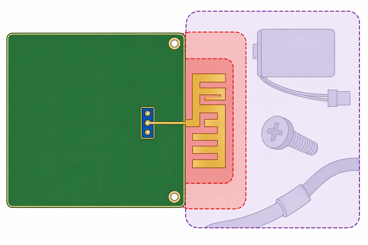
Place the antenna at a board edge or corner specified by the selected reference topology. Treat the radiator and its ground plane as one system. The ground is not merely a noise sink behind the radio; its size, edge and current distribution affect antenna behavior. Likewise, an antenna keepout is not decorative whitespace. It is a controlled three-dimensional region that must survive schematic review, placement, routing, copper-pour regeneration and mechanical integration.
Create named CAD regions for the radiator copper, feed transition, ground boundary and keepout. Apply the required exclusion to every copper layer when the selected reference calls for it. Keep ground pours, traces, vias, components and test pads out of that region unless the reference design explicitly includes them. Add a mechanical keepout for batteries, shields, displays, metal labels, screws, wiring harnesses and enclosure features. Put these constraints in the board notes and mechanical exchange, not only in an engineer’s memory.
Do not add a generic via fence around the radiator. Ground stitching may be appropriate along the RF feed or ground boundary when supported by the reference layout, but vias placed in the antenna field can change the structure. Reproduce the reference geometry or re-simulate and measure the change.
Route the RF Feed and Place a Configurable Matching Network
Route the radio output to the antenna through the shortest practical, uninterrupted reference structure supported by the radio reference design. Keep the reference plane continuous under a microstrip or grounded coplanar waveguide feed as applicable. Avoid unnecessary layer changes, stubs and discontinuities. If a transition is unavoidable, design it as an RF structure rather than treating it as an ordinary signal via.
There is no universal 50-ohm trace width. Width depends on the actual dielectric thickness, material properties, copper thickness, solder mask and whether the geometry is microstrip, stripline or coplanar. Calculate an initial width from the controlled fabrication stackup, then have the fabricator confirm the construction and impedance method. A calculator is an estimate; a field solver or fabricator model may be needed when geometry is tight or uncertainty matters.
Place a configurable matching network between the radio feed and radiator at the location recommended by the device or antenna supplier. A common development footprint can support series and shunt elements, but the initial population and topology must come from the applicable reference design. Keep pads compact and the shunt return short. Document unpopulated positions so assembly does not silently substitute a default network.
Keep Product Mechanics Out of the Antenna’s Unknowns
RF validation must follow the product configuration. A board tuned in open air can move when placed beside a battery or inside a plastic enclosure. A cable may act as an unintended counterpoise. A metal fastener or display frame can introduce loss or shift resonance. A hand or body can detune a handheld or wearable device. These effects are not reliably fixed by adding a capacitor after layout without first identifying the changed geometry.
Build a product-state matrix before the first RF test. Include at least the bare board, the intended enclosure, minimum and maximum battery or cable configurations, normal mounting hardware and realistic user-proximity states when applicable. Record which states are production-valid and which are diagnostic only. Use the same orientation, cable routing and measurement fixture when comparing revisions.
If mechanics cannot honor the antenna keepout, return to the implementation decision. A spring, wire, chip or external antenna may be more robust than compressing a printed pattern into an uncontrolled corner. That is an engineering trade, not a failure of PCB aesthetics.
Tune the Assembled Board with a Calibrated VNA Workflow
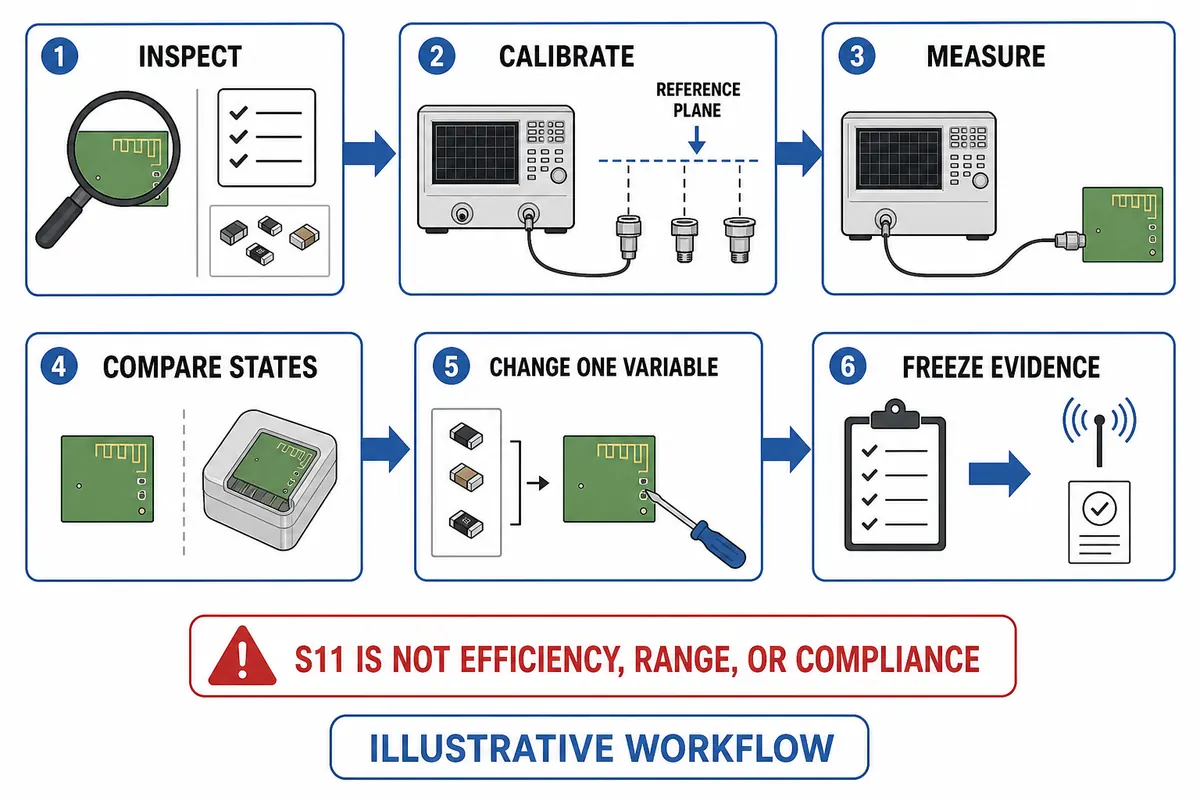
Plan the measurement connection before releasing the PCB. Define where the calibration reference plane will be and how the VNA will connect without leaving a long cable, adapter or unmodeled stub inside the antenna system. Depending on the design, this may use a suitable RF connector, a controlled fixture or a documented de-embedding method. The connection itself can disturb a compact antenna, so record it as part of the test configuration.
- Inspect the fabricated stackup, antenna copper, ground boundary, keepout and matching population against released data.
- Calibrate the VNA for the intended frequency span at the defined reference plane using the correct calibration method and standards.
- Measure the baseline board in a repeatable physical setup and save the trace, Smith chart data, fixture description and product state.
- Compare the observed response with the intended band and the reference design or simulation. Do not diagnose from resonance frequency alone.
- Change one controlled variable at a time: a designated trim feature, a matching element or a documented mechanical condition.
- Repeat the required enclosure, battery, cable and user-proximity states after selecting a candidate match.
- Freeze the final copper revision, matching BOM options, measurement record and radiated/compliance validation plan.
Stop matching and revisit the geometry if reasonable component changes produce a narrow, unstable or loss-dominated response; if the antenna depends on an uncontrolled cable or fixture; or if production tolerances move the result outside the required margin. A good impedance match created by dissipating energy is not a good antenna.
Diagnose Common 433 MHz Antenna Failures
| Observed symptom | Check first | Possible next action |
|---|---|---|
| Resonance shifted after enclosure assembly | Battery, plastic thickness, metal hardware, display and cable position | Restore mechanical clearance, compare controlled states, then retune representative hardware |
| Good bench S11 but poor range | Fixture/cable contribution, efficiency, pattern, orientation, receiver sensitivity and test method | Run separate radiated or comparative testing; do not infer radiation from S11 alone |
| Large unit-to-unit frequency spread | Stackup tolerance, antenna etch, solder mask, matching parts and enclosure assembly | Measure controlled coupons/boards and tighten only the variables shown to matter |
| Response changes when touching the cable | Calibration plane, common-mode current and connector/fixture geometry | Improve the measurement interface and repeat with controlled cable placement |
| No practical component match | Wrong reference layout, broken ground/keepout, excessive compacting or nearby conductor | Correct geometry or choose another antenna path instead of stacking extreme matching values |
| Passed prototype, failed production build | Fabricated stackup, BOM substitution, copper revision and mechanical configuration | Compare as-built evidence with the qualified configuration before changing the antenna |
Each symptom can have more than one mechanism. Use measurements to narrow the problem rather than treating this table as a universal diagnosis.
Apply a Source-Bounded Compact-Antenna Case
A published IEEE paper, “A Compact PCB Antenna for 433 MHz Band: Design, Simulation, and Experimental Validation,” reports a compact meandered structure with a shorting pin and describes simulation plus experimental validation. The case is useful because it treats compactness as a co-designed electromagnetic geometry and verifies the built antenna instead of presenting a trace-length rule.
The reusable lesson is the method: define the ground and board, model the complete structure, fabricate the documented geometry, measure it and compare the result. The reported dimensions and performance belong to that paper’s construction and test conditions. They are not PCBtry customer data, not a universal 433 MHz pattern and not permission to copy the design into a different enclosure or stackup.
Release the Layout Only with Documented Evidence
Before CAD release, package the information another engineer needs to reproduce and verify the antenna: radio and reference design revision, intended market, actual stackup, antenna topology, ground dimensions, all-layer keepout, mechanical exclusion, feed geometry, matching footprint and population options, measurement connector or fixture, product-state matrix and the owner of radiated and compliance testing.
Use the 433 MHz PCB Antenna Layout and Tuning Worksheet to record these items. It is an original PCBtry engineering work aid based on the cited sources. It is not an antenna reference design, simulation report, chamber report, certification plan or proof that a product complies.
For broader terminology, see the PCB antenna fundamentals guide. For stackup-dependent RF routing context, review high-frequency PCB design guidelines. When preparing manufacturing data, use the PCB placement, routing and DFM workflow to keep antenna constraints visible through release.
433 MHz PCB Antenna Layout FAQs
How long should a 433 MHz PCB antenna be?
A free-space quarter wavelength is about 173 mm, but that is a scale reference rather than a universal printed length. Use the selected reference design, actual stackup and board geometry to establish an initial shape, then tune representative hardware.
Can I fold a 173 mm trace into a small meander?
Not by path length alone. Adjacent segments couple, the ground participates and compacting can change loss and bandwidth. Treat the meander as an electromagnetic structure that needs simulation or a validated reference plus measurement.
Should there be ground copper under a 433 MHz PCB antenna?
Follow the exact topology. Many printed or chip-antenna references require a copper-free region under and around the radiator while using a defined ground plane elsewhere. Do not apply a universal ground-under or no-ground rule.
How large should the antenna keepout be?
Use the selected antenna or radio reference layout as the starting requirement. Document copper and mechanical keepouts separately, because batteries, shields and enclosure hardware can matter even when they are not on the PCB.
What is the correct 50-ohm trace width?
It depends on the real stackup, dielectric properties, copper, solder mask and transmission-line geometry. Calculate it from the controlled stackup and confirm it with the fabricator or an appropriate solver.
Do I need a matching network?
Provide the configurable footprint required by the reference design. Final values must be determined on representative hardware; copying values from another board assumes the two antenna systems are equivalent.
Can a NanoVNA tune a 433 MHz antenna?
A suitable calibrated VNA can measure impedance and reflection around 433 MHz, but the fixture and calibration plane must be controlled. The result does not independently prove radiation efficiency, range or compliance.
Why does the antenna change when the enclosure is fitted?
The enclosure, battery, wiring, display, metal parts or user proximity can change fields and loss. Compare controlled product states and correct the mechanical or antenna design before accepting a final match.
Does good S11 guarantee long range?
No. S11 describes reflection at a reference plane. Range also depends on radiation efficiency and pattern, transmit power, receiver sensitivity, orientation, propagation, interference, protocol and the test method.
Is 433 MHz licence-free everywhere?
No universal permission exists. Frequency availability, power, duty cycle, bandwidth and application conditions depend on the jurisdiction and current rules. Confirm the target market with the applicable regulator or qualified compliance resource.
Prepare the Board for Fabrication and RF Validation
Before requesting a fabrication review, provide the Gerbers or ODB++ data, controlled stackup, antenna reference source, board and ground dimensions, keepout drawing, matching options, enclosure model and planned RF test connection. Ask the fabricator to confirm stackup and impedance assumptions. Keep antenna tuning, radiated performance and regulatory approval assigned to qualified owners; fabrication conformity alone does not prove them.
If you need PCB manufacturing feedback, share the actual data package with PCBtry and request confirmation of the stackup, controlled-impedance construction, copper features, solder-mask treatment and mechanical tolerances that affect your RF validation plan.
Sources and Scope
- Texas Instruments SWRA161B, ISM-Band and Short Range Device Antennas
- Texas Instruments SWRA351, Antenna Selection Quick Guide
- Silicon Labs AN853, Antenna Matching
- Microchip AT02865, RF Layout with Microstrip
- 47 CFR 15.231
- A Compact PCB Antenna for 433 MHz Band: Design, Simulation, and Experimental Validation



0 Comments