




An A4988 PCB layout is not a generic “put the driver near the motor connector” exercise. The device regulates two winding currents with switching full bridges, measures those currents through SENSE1 and SENSE2, and moves heat through a 5 mm × 5 mm exposed-pad QFN. Placement has to preserve those electrical and thermal paths before routing begins.
This guide is for a custom board that mounts the Allegro A4988 IC. If your motherboard only accepts a Pololu-, StepStick-, or Adafruit-style carrier, use the carrier vendor’s footprint, pinout, keepout, power-input, and cooling instructions. A carrier already owns the chip-level sense resistors, charge-pump capacitors, exposed-pad layout, and much of the thermal design.
The device-specific statements below are grounded in the Allegro A4988 datasheet, revision 8 dated April 5, 2022. General routing and prototype checks are engineering guidance, not guarantees. Confirm the current datasheet, orderable part, stackup, copper weight, assembly process, load profile, ambient temperature, and enclosure conditions for your project.
First Decide: Bare A4988 IC or Plug-In Carrier Module?
The two design paths share a part name but not the same PCB task.
| Decision | Bare A4988 on your PCB | Plug-in carrier on your PCB |
|---|---|---|
| Footprint | Allegro ET 28-contact QFN land pattern and assembly rules | Carrier header pattern, board outline, insertion clearance, orientation, and vendor keepouts |
| Current regulation | You select and lay out RS1, RS2, VREF circuitry, and ROSC configuration | The module owns the sense resistors and usually provides a current-adjustment method |
| Local support parts | You place VBB/VDD bypass, charge-pump, and VREG components | Verify which parts are already fitted; add only the motherboard-level supply network the vendor requires |
| Thermal path | Your exposed-pad land, solder process, vias, planes, and airflow control junction temperature | The module controls chip-to-carrier heat flow; your motherboard and airflow still affect the module environment |
| Source of truth | Allegro datasheet plus your fabricator’s QFN capability | Exact module manufacturer’s schematic, dimensions, revision, and user guide |
Do not copy a carrier’s advertised current, copper weight, bulk capacitor, or thermal result into a bare-chip specification. For example, Pololu publishes resources and performance notes for its own A4988 carrier, while Adafruit publishes Eagle schematic and board files for its breakout. Those are valuable examples, but their results belong to those boards and test conditions.
Freeze the A4988 Package, Datasheet Revision, and Current Assumptions
Allegro’s current datasheet identifies the A4988SETTR-T in a 28-contact ET QFN with an exposed thermal pad. The package section gives a reference land pattern and states that the drawing is for reference, not tooling. Create or approve the CAD footprint against that source and your assembly supplier’s paste, solder-mask, via-in-pad, and inspection capability. A footprint copied from an anonymous library is not verified because it passes DRC.
Record the motor-supply range and transients; logic supply and I/O levels; target winding current, microstep modes, duty cycle, and acceleration profile; sense-resistor value, tolerance, power rating, package, and temperature behavior; VREF source and range; layer count, finished copper, allowable temperature rise, ambient, enclosure, and airflow; and connector current rating and cable direction.
The datasheet relates the maximum trip current to reference voltage and sense resistance as ITripMAX = VREF / (8 × RS). That equation is a starting point, not a complete thermal qualification. It does not prove that the IC, resistor, connector, copper, or enclosure can continuously support the calculated current.
Place the A4988 Around Its Functional Current Loops
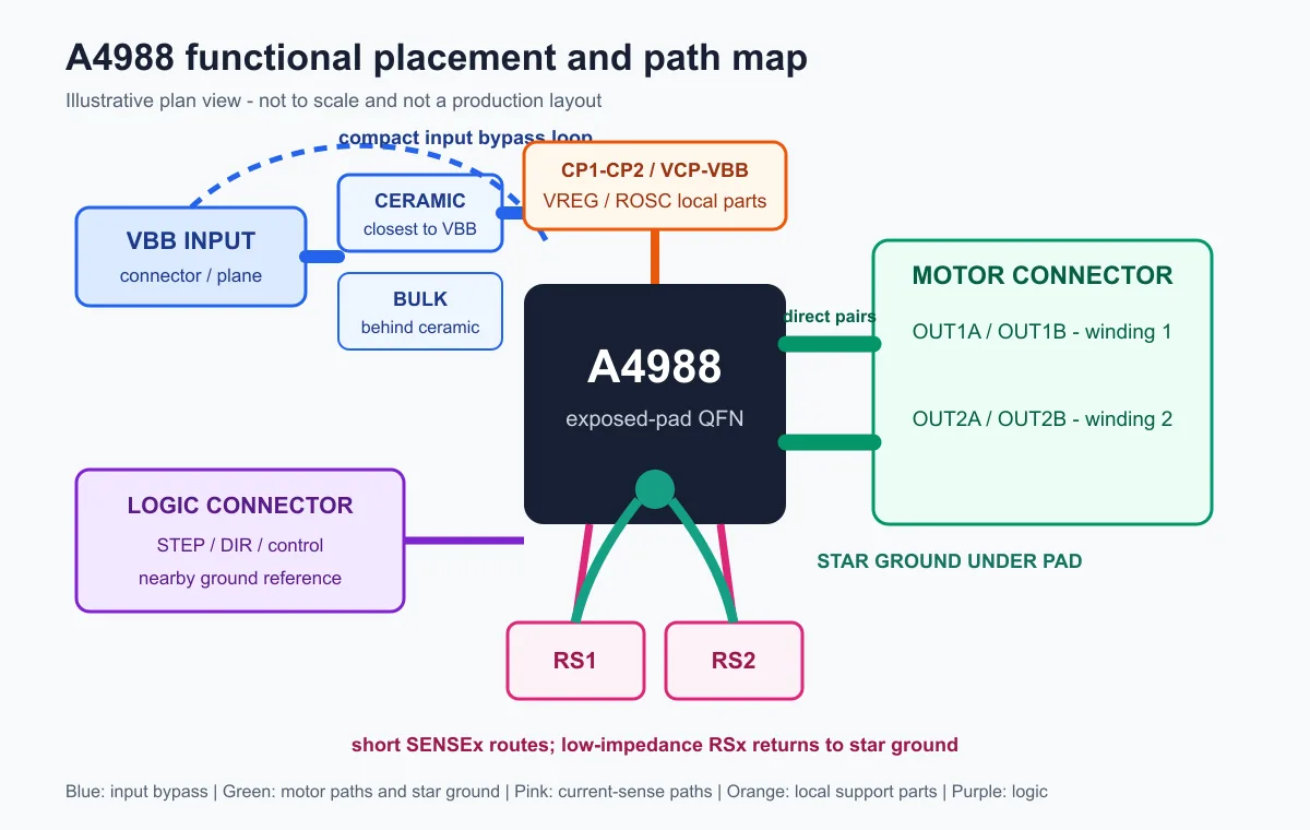
Place the QFN first, then reserve its exposed-pad copper and assembly geometry. Arrange components by the path they serve instead of by reference-designator order:
- Input loop: VBB connector or distribution plane, ceramic bypass, both VBB pins, ground return, and nearby bulk capacitance.
- Bridge paths: VBB1/2 through the internal bridges to OUT1A/1B and OUT2A/2B, the motor connector, windings, and sense-resistor return.
- Measurement paths: SENSE1/2 to RS1/2 and then to the low-impedance star-ground region.
- Gate-drive support: CP1–CP2, VCP–VBB, and VREG-to-ground capacitors.
- Control paths: STEP, DIR, RESET, SLEEP, ENABLE, MS1–MS3, VREF, ROSC, VDD, and their returns.
Keep enough room to route these groups without necking down current paths or cutting the ground plane into accidental islands. This is why a placement plan should precede routing; see PCBtry’s guide to PCB placement, routing, and DFM checks.
Route the VBB Input Loop and Motor Outputs
Allegro calls for two input capacitors in parallel and places the ceramic capacitor closer to the supply pins than the bulk capacitor. The ceramic part supplies the high-frequency current component. Route its VBB-to-ground loop compactly, using a short connection to both supply pins and the nearby ground region. Place bulk energy storage close enough to support the local supply without forcing ceramic-capacitor current through a long shared path.
Do not choose a motor-output width from a screenshot. Width depends on finished copper, allowable rise, length, layer, adjacent copper, airflow, terminal geometry, and current waveform. Document the calculation and ask the fabricator to confirm finished copper assumptions. PCBtry’s copper-thickness review guide explains why nominal copper weight alone does not establish a current rating.
Route each motor pair so the path to its connector is direct and does not force switching current through the logic-ground area. Avoid narrow necks at pads, thermal-relief spokes, vias, and connector entries. If a layer transition is unavoidable, size and distribute vias from a documented current and fabrication calculation rather than a memorized count.
Keep SENSE1 and SENSE2 Out of the Switching-Current Path
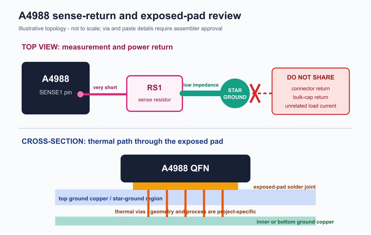
The sense resistors carry winding current and also create the voltage that the comparators measure. Allegro warns that a long ground trace adds voltage drop and degrades current measurement. Its Figure 8 shows very short SENSEx connections to RSx and thick, low-impedance connections from the resistors to the star ground under the device, with no other components in the sense circuits if possible.
- The SENSEx pin should reach its resistor without sharing a segment with an unrelated load.
- The resistor’s ground side should reach the star-ground region without carrying connector, bulk-capacitor, logic, or other-channel current first.
- The resistor footprint, copper, and solder joints must support calculated dissipation and measurement accuracy.
Do not call this a “Kelvin connection” unless the actual footprint and geometry implement one. The observable goal is that bridge current does not create an uncontrolled shared voltage drop in the comparator’s measurement path. The datasheet also states that SENSE1 and SENSE2 must not exceed their 0.5 V maximum rating.
Keep Charge-Pump, VREG, and ROSC Parts at Their Assigned Pins
The charge pump drives the high-side FET gates. Allegro specifies a 0.1 µF ceramic capacitor between CP1 and CP2 and another 0.1 µF ceramic reservoir between VCP and VBB. VREG requires a 0.22 µF ceramic capacitor to ground. The datasheet also specifies dielectric and tolerance conditions. Use the values and conditions from the revision you approve, then place each loop at its assigned pins before less critical passives.
ROSC is a configuration node. The datasheet documents connections to VDD, ground, or a resistor to ground, with decay-mode or off-time consequences. Choose from motor-behavior requirements, keep the connection local, and record the selected mode. Do not add a long test trace or noisy shared route without analyzing its effect.
Connect the Exposed Pad to a Low-Impedance Ground and Thermal Path
Allegro calls for a heavy ground plane and a low-impedance single-point ground close to the device. It identifies the region directly under the A4988, where the pad connects to the ground plane, as the star-ground location. Package notes add that thermal vias in the exposed-pad land can improve dissipation on a multilayer PCB.
Those statements define topology, not a universal via recipe. Via diameter, pitch, fill or cap process, paste-window design, voiding target, copper distribution, and inspection method belong to the board and assembly process. Confirm them with the assembler. Too little solder can weaken the thermal joint; excessive open via-in-pad area can drain solder.
Do not use the datasheet’s 32 °C/W four-layer JEDEC thermal-resistance value as a prediction for your board. It is tied to standard test conditions. Estimate losses for the planned waveform, then validate device temperature across realistic voltage, motion, ambient, enclosure, and airflow. PCBtry’s discussion of how PCB layout changes the heat path can help structure that review.
Give Every Logic Input a Defined State and Return Path
Route STEP and DIR away from motor outputs and keep a continuous reference beneath them. The datasheet specifies 1 µs minimum high and low STEP pulse widths and 200 ns setup and hold times for relevant input changes around STEP. These limits belong in the interface and firmware review; they do not justify routing beside switching nodes.
RESET, SLEEP, ENABLE, and MS1–MS3 need intentional states during controller reset, boot, connector removal, and fault recovery. Do not assume pull resistors found on a carrier exist inside a bare-IC design. Verify pin descriptions and add biasing where the system requires it. Give logic connectors nearby ground references so return current does not search through the motor-power region.
After SLEEP returns high, Allegro specifies a 1 ms delay before a STEP command so the charge pump can stabilize. Include that requirement in firmware and bring-up evidence.
Run a Net-by-Net Review Before Gerber Release
Download the A4988 PCB Layout Review Checklist (PDF). This two-page blank worksheet is an original PCBtry editorial aid based on the cited Allegro datasheet. It is not an Allegro document, completed test record, customer file, safety approval, design certification, or proof of compliance.
| Network | Layout evidence to show | Failure to investigate | Stop condition |
|---|---|---|---|
| VBB1/VBB2 and input capacitors | Ceramic closest to pins; compact VBB-ground loop; bulk path visible | Supply bounce, heating, resets, excessive ringing | Return path crosses a split or narrow neck |
| OUT1A/B and OUT2A/B | Direct paired routes, connector rating, width/via calculation | Copper or connector heating, coupling into logic | Rating depends on undocumented copper |
| SENSE1/2 and RS1/2 | Short sense path and low-impedance resistor return to star ground | Wrong trip current, mismatch, noise-sensitive regulation | Unrelated current shares measurement return |
| CP1/CP2, VCP, VREG | Correct capacitor values and pin-adjacent loops | Gate-drive or regulator fault | Value, dielectric, or destination net is unverified |
| Exposed pad and ground | Pad land, plane connection, via/process drawing, paste review | Ground bounce, solder voiding, high junction temperature | Assembler has not approved the process |
| Logic and VREF/ROSC | Defined states, continuous reference, selected mode, safe test points | Unexpected startup, wrong decay mode, false steps | Carrier defaults were assumed for a bare IC |
A credible release package includes the approved schematic, exact datasheet revision, stackup, finished-copper requirements, current and thermal calculations, footprint source, DRC report, assembly notes, and a marked-up layout showing critical paths. A screenshot without nets or assumptions is not review evidence.
Validate the Prototype With a Controlled Current Ramp
Use a current-limited bench supply and begin with outputs disabled. Confirm no shorts, correct logic supply, expected states, and a safe VREF range before enabling the bridge. Connect the intended motor and increase the target in controlled steps while observing supply current, sense behavior with an appropriate method, motor behavior, and component temperatures.
This is general lab guidance, not a substitute for a project test plan. Probe switching circuits only with instruments, grounding, isolation, and training suitable for the voltage and transients. Stop if measured sense behavior disagrees with the VREF/RS calculation, the supply is unstable, the IC repeatedly enters protection, a connector or resistor heats unexpectedly, or junction-temperature margin cannot be demonstrated.
A useful public reference scenario is Allegro’s Figure 8. It addresses a specific problem: long sense-ground traces add voltage drop that corrupts measurement. The documented treatment is a short SENSEx-to-RSx connection and a thick, low-impedance resistor return to star ground under the device. The action for your board is to highlight both paths in CAD and confirm no other load shares them. The sought result is not a promised temperature or current; it is a topology matching the manufacturer’s guidance. This is a datasheet-derived review example, not a PCBtry customer case or test result.
A4988 PCB Layout FAQ
Can I copy a Pololu or Adafruit A4988 carrier layout?
You may study vendor-published files under their licenses, but do not assume their current, thermal, connector, copper, or component choices fit your board. Start with Allegro and document changed conditions.
Does an A4988 PCB need a ground plane?
Allegro calls for a heavy ground plane and low-impedance star ground close to the device. Implement that topology without cutting critical returns, then verify it against your stackup.
Where should the A4988 input ceramic capacitor go?
Place it closer to the VBB pins than the bulk capacitor, as Allegro specifies, and minimize its VBB-to-ground loop.
How should I route A4988 sense resistors?
Keep each SENSEx connection to RSx very short and connect the resistor to star ground with a thick, low-impedance path. Avoid unrelated current in that circuit.
How wide should A4988 motor traces be?
There is no universal width. Calculate from waveform, finished copper, layer, length, allowable rise, vias, connector, ambient, and cooling, then confirm fabrication assumptions.
How many thermal vias should go under the A4988?
The datasheet says vias can improve dissipation but gives no universal count. Coordinate land, via, paste, fill/cap, voiding, and inspection rules with the assembler.
Can I use the 2 A absolute rating as a continuous current?
No. An absolute maximum is not a guaranteed operating point. Continuous capability depends on losses, PCB thermal path, ambient, airflow, enclosure, waveform, and junction-temperature margin.
Should analog and power grounds be split?
Do not apply a generic split-ground rule. Follow Allegro’s low-impedance star-ground topology and trace actual high-current and measurement returns.
What should I check around ROSC?
Choose a datasheet-defined ROSC configuration for the required decay/off-time behavior, place it locally, and record the selected mode.
What proves an A4988 layout is ready?
No single DRC result proves readiness. Require source-verified footprint and support parts, visible current and return paths, calculations, assembler-approved exposed-pad processing, and prototype validation.
Prepare the Evidence a PCB Manufacturer Needs
Before requesting a quote or DFM review, send the stackup target, finished copper, Gerbers or ODB++ data, drill files, IPC-356 netlist if available, BOM, centroid data, assembly drawing, package source, exposed-pad and paste notes, current assumptions, and the marked-up critical-path review. Flag sense resistors, motor connectors, high-current vias, and the thermal-via process instead of expecting the manufacturer to infer their purpose.
PCBtry can review the fabrication and assembly handoff against the requirements you supply. The design owner remains responsible for circuit function, safety limits, current setting, thermal validation, and regulatory requirements. Submit the actual stackup, load profile, copper assumptions, and assembly constraints so the review is evidence-based rather than a generic A4988 template.
Primary and example sources
- Allegro MicroSystems, A4988 Datasheet, Rev. 8 — primary device, application-layout, package, timing, and current-regulation source.
- Allegro A4988 product page — current manufacturer document hub.
- Adafruit A4988 breakout design files — traceable board example, not a universal layout.
- Pololu A4988 carrier resources — carrier-specific schematic, mechanical, and operating resources.



0 Comments