




AI can already assist parts of PCB layout, but “AI for PCB layout” is not one capability. It may mean a conversational assistant that explains a rule, a checker that prioritizes warnings, an optimizer that explores placement candidates, an autorouter, or a service that generates complete layout candidates. Those systems accept different inputs and produce different evidence. Treating them as interchangeable is the fastest way to mistake an attractive board view for a release-ready design.
A safer question is: which bounded layout task can the tool perform, which constraints can it actually read, and what independent evidence will decide whether its output is acceptable? This guide gives PCB designers and hardware leads a practical way to answer that question. Product capabilities are described from official documentation available in August 2026; availability and commercial terms can change.
Where AI Fits in the PCB Layout Workflow
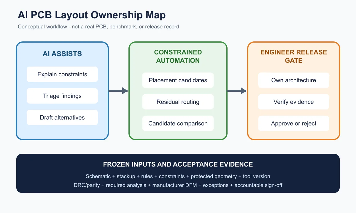
Start by identifying the kind of automation you are evaluating. A tool that answers a question about a datasheet is not equivalent to a placement optimizer, and neither is equivalent to a constraint-driven routing engine.
| Capability class | Typical output | What still needs proof |
|---|---|---|
| Conversational assistant | Explanations, proposed rules, component or workflow suggestions | Source accuracy, correct interpretation, and approval of every applied change |
| Review assistant | Prioritized warnings or suggested fixes | Check coverage, false positives, false negatives, and the correctness of each fix |
| Placement optimizer | One or more component arrangements | Mechanical constraints, functional grouping, routing feasibility, thermal path, and service access |
| Routing automation | Tracks, vias, fanout, or route candidates | Constraint coverage, return paths, topology, impedance, coupling, current capacity, and manufacturability |
| End-to-end candidate generator | Native PCB files or manufacturing outputs | Everything required by the release process, including independent analysis and accountable sign-off |
Current products illustrate this range. Flux documents an AI Auto-Layout feature that starts from placement and constraints, generates iterations, and protects existing traces; its own guidance recommends routing critical signals manually first and reviewing the result. Cadence describes AI-enabled placement, constraint-driven routing, and integrated multiphysics exploration in Allegro AI Studio. Quilter describes a candidate-generation workflow using uploaded Altium or KiCad files plus user-defined physics constraints. These are useful examples of advertised scope, not a universal ranking or proof that one workflow fits every board.
The distinction matters because conventional deterministic automation is often grouped under the AI label. Interactive routing, design-rule checking, length tuning, and schematic-layout synchronization remain valuable whether or not machine learning is involved. The practical measure is not the label. It is whether the system preserves design intent and produces reviewable evidence.
The Constraints AI Needs Before Placement or Routing
An optimizer cannot honor a requirement it cannot see. Before the first run, convert design intent into explicit, reviewable inputs. This is also sound practice for a manual PCB layout workflow.
- Board and mechanical limits: outline, cutouts, connector locations, mounting holes, height limits, keepouts, enclosure walls, assembly access, and test access. If these are absent, a compact placement may be mechanically impossible.
- Approved stackup and fabrication capability: layer count, copper weights, dielectric targets, via types, drill limits, annular rings, trace/space limits, and impedance process. A geometric route can be invalid when evaluated against the actual fabricator’s process.
- Electrical classes: voltages, currents, minimum widths, clearances, creepage, differential-pair rules, length limits, skew limits, and allowed layer transitions. A default rule set rarely represents the whole product.
- Topology and path intent: source-load order, termination location, star points, sensing points, current loops, controlled return paths, isolation barriers, and nets that must not share copper or return geometry. A netlist describes connectivity, not all physical intent.
- Placement intent: fixed parts, functional groups, decoupling relationships, noisy and quiet regions, thermal interfaces, antenna or sensor keepouts, and orientation requirements.
- Verification scope: the checks, analyses, models, manufacturing rules, and reviewer approvals that define success.
Official KiCad documentation makes the rule-coverage problem visible: DRC severities are configurable and individual checks can be ignored. Altium’s documentation likewise emphasizes that routing is rule-driven and rules should be configured before routing. Therefore, “the tool followed the rules” is only useful after someone confirms which rules existed, how they were scoped, and whether any were disabled or excluded.
AI PCB Layout Task Matrix: Low-Risk, Conditional, and Human-Owned
Choose a first task by the consequence of failure and the strength of independent verification—not by how impressive the demo looks.
| Task | Suggested ownership | Minimum controls | Reason |
|---|---|---|---|
| Explain a rule or draft a review question | AI-assisted | Link to authoritative documentation; engineer checks the interpretation | Easy to review before it changes the board |
| Classify DRC findings or suggest likely causes | AI-assisted | Keep original DRC evidence; approve fixes individually; rerun checks | Useful for triage, but a suggestion can be wrong |
| Place repeated low-risk circuitry | Conditional automation | Locked mechanical anchors, placement rules, baseline comparison, routing review | Repetition is measurable, but local placement affects global routing |
| Route noncritical residual nets | Conditional automation | Critical nets pre-routed or protected, complete rules, DRC and visual return-path review | A bounded residual task limits the failure surface |
| Choose stackup, partitioning, grounding architecture, or safety strategy | Engineer-owned | System requirements, analysis, supplier data, and accountable design review | These are coupled architectural decisions, not merely geometry |
| Release fabrication data | Engineer-owned approval | Complete verification record, controlled revision, manufacturer DFM, and sign-off | The release decision carries product and manufacturing risk |
Research supports this bounded-task view. Published work explores PCB fanout, placement, routing, and net-ordering subproblems. That is meaningful progress, but a specialized benchmark result is not evidence that every constraint of an arbitrary product has been captured. PCB-Bench, an ICLR 2026 benchmark, reports substantial gaps in current LLM spatial reasoning, constraint following, and interpretation of professional PCB artifacts. The right conclusion is not that AI has no value; it is that task scope and verification strength must grow together.
Why Critical Nets and Physical Architecture Still Need an Engineer
Critical layout decisions combine requirements that may not exist in the netlist or rule database. A switching converter hot loop depends on topology, switching edges, component parasitics, copper geometry, and return-path area. A high-speed interface depends on the approved stackup, reference continuity, transitions, coupling, discontinuities, and receiver requirements. An RF feed, precision sense path, isolation barrier, or high-current connection has similarly coupled behavior.
An AI system can propose geometry, but the engineer must decide whether the objective function represents the real failure modes. Shorter total wirelength, fewer vias, or 100% routing completion can be useful metrics; none proves the correct return path, acceptable emissions, stable power delivery, safe creepage, reliable thermal behavior, or testable assembly.
Route or lock critical geometry before delegating residual work when the tool supports that pattern. Flux’s official Auto-Layout guidance, for example, says existing tracks can be protected and recommends manually routing important signals first. This is a product-specific workflow example, not a universal guarantee. In every tool, verify exactly what is frozen and what the engine is allowed to move.
A Controlled Pilot for AI-Assisted PCB Layout
Use a representative but low-consequence board or functional block. Do not begin with the company’s most complex, safety-critical, RF-sensitive, or schedule-critical design.
- Write the hypothesis. Example: “For this already placed two-layer control board, the tool can route the noncritical residual nets without changing protected power and clock routes, while meeting the frozen rule set.” This is a hypothetical test statement, not a performance claim.
- Freeze inputs. Archive the schematic, PCB, libraries, stackup, rules, constraints, tool version, and any prompts or job settings.
- Keep a baseline. Use an engineer-reviewed manual or interactive-routing version of the same input. Do not compare different schematics or changing rule sets.
- Define pass/fail gates before the run. Include routing completion, zero unapproved DRC violations, schematic parity, protected-object integrity, required analysis, and reviewer sign-off.
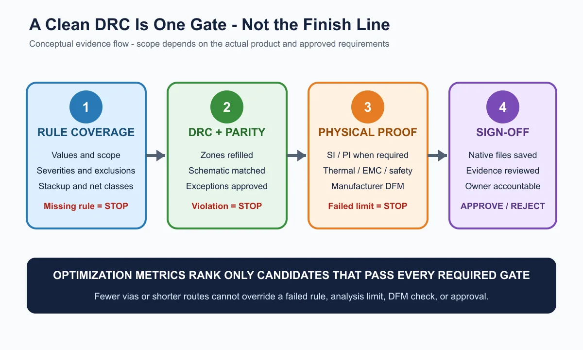
- Define optimization metrics separately. Examples include via count, total route length, critical-net margin, estimated fabrication difficulty, review time, and number of manual corrections. These help rank passing candidates; they must not override a failed gate.
- Run and preserve candidates. Save native editable files, not screenshots alone. Record rejected candidates and why they failed.
- Stop when evidence is inadequate. Abort if a critical constraint cannot be encoded, the tool changes protected objects, results are unstable, native output is unavailable, or reviewers cannot explain the geometry.
Real Case: Separate Raw AI Output From the Fabricated Revision
Quilter’s published Project Speedrun design-file package provides a useful real-world audit pattern. The company reports using its system on a two-board, eight-layer i.MX 8M Mini Linux computer with 843 components and 5,141 pins. More important for evaluation, the download separates three states for each board: the input supplied to the tool, the raw AI-generated output before human cleanup, and the final cleaned-up revision sent to the manufacturer.
Problem: a complex multi-board computer required a complete physical layout. Treatment: the vendor used its constraint-driven generation workflow and then performed human cleanup before fabrication. Action: it released input, raw-output, and fabricated-revision files so reviewers can inspect what automation produced and what changed before release. Reported result: Quilter states that the fabricated computer booted on its first attempt and reports about 38.5 hours of human engineering effort versus a 428-hour professional layout quote.
Those numbers are vendor-reported results from one project, not an independent benchmark or a promise for another board. A first boot also does not, by itself, prove every reliability, EMC, safety, thermal, or production requirement. The reusable lesson is the evidence structure: preserve the raw candidate, preserve the human-modified release, and review the delta. If a case study shows only the polished final board, readers cannot tell which decisions came from automation and which came from engineers.
Why a Clean DRC Report Is Not Enough
DRC is necessary. It is also bounded by configuration. A clean report can coexist with an incorrect design when a clearance value is wrong, a rule is scoped to the wrong objects, an exception is stale, a severity is set to ignore, zones were not refilled, or the PCB no longer matches the schematic.
KiCad documents both electrical and design-for-manufacturing checks and warns that ignored severities disable checks. It can also test schematic parity and produce a command-line DRC report, which is useful for a reproducible pilot. Those reports establish compliance with the configured checks. They do not replace:
- signal-integrity review or simulation for applicable interfaces;
- power-integrity and voltage-drop analysis where current paths matter;
- PCB thermal-path analysis and temperature validation;
- EMC pre-compliance reasoning or measurement;
- safety, isolation, and regulatory assessment;
- assembly access, testability, component availability, and manufacturer-specific DFM;
- prototype bring-up and product-level verification.
When a vendor describes integrated multiphysics optimization, verify which solver, model, boundary conditions, material properties, and sign-off criteria were actually used. “Physics-driven” is a useful direction, but it is not a substitute for a reviewable analysis setup and result.
AI Layout Candidate Scorecard
Separate release gates from ranking metrics. A candidate that fails one mandatory gate should not win because it has fewer vias.
| Evidence item | Gate or metric? | Record |
|---|---|---|
| Input revision and tool/version identity | Gate | Hashes or controlled revision IDs; settings and prompt/job record |
| Schematic-layout parity | Gate | Report and unresolved differences |
| DRC configuration and result | Gate | Rule set, severities, exclusions, report, and approved exceptions |
| Protected critical geometry unchanged | Gate | Diff review or object comparison |
| Required SI/PI, thermal, EMC, safety, or DFM result | Gate | Analysis setup, result, limit, and reviewer |
| Unrouted nets, via count, route length, or correction count | Metric | Comparable values from the same frozen inputs |
| Exception disposition | Gate | Accept, revise, or reject with an accountable owner and reason |
Download the AI PCB Layout Evaluation Worksheet (PDF) to record constraints, gates, candidate metrics, and dispositions. This original source-based file is an editorial planning aid. It is not a design standard, test report, customer record, simulation result, compliance certificate, manufacturer approval, or proof that a board is production-ready.
PCB Design IP and Cloud AI Questions
Schematics, layouts, BOMs, constraints, simulation models, and fabrication notes may reveal product architecture and supplier strategy. Before uploading them to any cloud AI or routing service, obtain answers from the provider’s current contractual and security documentation:
- Which files and derived data leave your environment?
- How long are inputs, outputs, logs, and backups retained?
- Can customer data be used to train or improve models, and can that use be disabled contractually?
- Who can access the project, and how are tenant isolation and access logs handled?
- Which regions process and store the data?
- What deletion mechanism and verification are available?
- Can you export complete native files, rule sets, history, and evidence without vendor lock-in?
- Does the workflow meet your organization’s export-control, confidentiality, customer, and regulatory obligations?
Do not infer favorable answers from the word “secure” on a marketing page. If the answers are incomplete, use sanitized nonproprietary test designs or keep the task inside an approved environment.
From AI Layout Candidate to Manufacturer Handoff
An acceptable candidate still needs controlled manufacturing information. Confirm the approved stackup, materials, copper weights, impedance requirements, drill and via definitions, finished thickness, surface finish, tolerances, special processes, panel or assembly constraints, fabrication notes, and every approved exception. Include the editable source and rule files needed for review, along with generated fabrication outputs and their revision identity.
Ask the selected manufacturer to review the real package rather than a screenshot or generic capability table. Manufacturing feedback may require geometry or stackup changes, which must return through the same controlled design and verification loop. PCBtry’s PCB design service can be used as a handoff discussion point, but project-specific capability, tolerances, materials, and verification requirements still need written confirmation.
AI for PCB Layout FAQ
Can AI design a complete PCB layout?
Some current tools advertise placement, routing, checking, or complete candidate generation. Whether a candidate is usable depends on the supplied constraints, board class, output fidelity, independent checks, and engineering sign-off. “Complete” must be defined by your release gate, not routing percentage alone.
Is AI PCB layout the same as an autorouter?
No. Autorouting is one form of layout automation. AI may also assist with questions, rule extraction, review, placement optimization, candidate ranking, or tool orchestration. Ask what algorithmic function is actually being performed and what evidence it returns.
Does zero DRC violations mean an AI layout is correct?
No. It means the board passed the enabled checks with their current values, scope, and exceptions. It does not by itself prove schematic parity, signal integrity, power integrity, thermal performance, EMC, safety, or manufacturer acceptance.
Which PCB layout tasks are safest to try first?
Begin with review assistance, documentation, or bounded repetitive work whose output is easy to compare and reverse. Noncritical residual routing can be a candidate when critical geometry is protected and the rule set is complete.
Should beginners use AI for PCB layout?
AI can explain concepts and expose alternatives, but beginners may not recognize a plausible-looking error. Use it with authoritative references, deterministic checks, and review by someone able to explain current paths, return paths, constraints, and manufacturing consequences.
Can AI route high-speed, RF, power, or precision analog nets?
A tool may generate geometry for these nets, but acceptance requires project-specific topology, stackup, return-path, coupling, current, thermal, and analysis evidence. Keep such decisions engineer-owned unless the exact constraints and verification chain are demonstrably covered.
How should AI layout tools be benchmarked?
Freeze identical inputs, rules, and objectives; preserve a reviewed baseline; define pass/fail gates before the run; and compare only candidates that pass. Record tool versions, reports, exceptions, manual corrections, and reviewer decisions.
Are cloud AI PCB tools safe for confidential designs?
That cannot be assumed. Review the provider’s current contract and security documentation for data use, retention, training, access, processing location, deletion, and export. Use sanitized designs when approval is absent.
Will a PCB manufacturer accept an AI-generated layout?
A manufacturer evaluates the actual design package against its process. The origin of the geometry does not remove the need for stackup, material, drill, tolerance, impedance, DFM, and revision-control information.
Will AI replace PCB layout engineers?
Current evidence supports automation of bounded tasks and faster exploration, while benchmarks still show gaps in spatial and constraint reasoning. Engineering responsibility shifts toward explicit design intent, verification, tradeoff review, and accountable release rather than disappearing.
Set the Acceptance Gate Before the First AI Run
Select one low-consequence board or block. Write down the frozen input revision, protected geometry, rule set, mandatory analyses, manufacturer constraints, pass/fail thresholds, evidence files, reviewers, and abort conditions. Only then run the tool.
If a candidate passes the gate and reduces effort without hiding decisions, expand the scope gradually. If the tool cannot represent a critical requirement or produce auditable native output, keep that task in the controlled interactive or manual flow. The goal is not to prove that AI can draw copper. It is to prove that your team can understand, verify, manufacture, and take responsibility for the result.
Sources and capability references
- Flux: AI-Powered Auto-Layout
- Flux: AI-Powered Design Reviews
- Cadence: Allegro AI Studio
- Quilter: How the Layout Workflow Works
- KiCad PCB Editor and DRC Documentation
- Altium: Defining and Scoping PCB Design Rules
- PCB-Bench: Benchmarking LLMs for PCB Placement and Routing
- FanoutNet: Neuralized PCB Fanout Automation
- Quilter Project Speedrun: Input, Raw AI Output, and Fabricated Revision



0 Comments