




A PCB schematic tells you the circuit’s intended electrical relationships. The physical board shows how one assembly was actually built. Cross-checking the two means proving correspondence with controlled evidence—not searching for shapes that look similar.
Start with the board identity and revision, then connect each conclusion to the appropriate source: schematic, bill of materials (BOM), assembly drawing, layout or netlist, manufacturer datasheet, visible board feature, or a bounded measurement. A top mark, silkscreen label, or continuity beep can support a conclusion, but none of them automatically proves the entire circuit.
Safety boundary: this guide emphasizes document review, visual inspection, and limited unpowered checks. Do not probe an energized assembly unless you are trained for the circuit’s voltage, energy, grounding, and measurement category and are using suitable procedures and equipment. Disconnect power and discharge stored energy before resistance or continuity measurements. When the board contains mains voltage, large capacitors, high-current batteries, or an unknown power section, stop and obtain qualified support.
What Can a Schematic Prove About a Physical PCB?
A schematic is a logical model. It shows symbols, pins, net labels, junctions, power domains, and functional relationships. The symbol positions are chosen for readability; they are not physical coordinates. A PCB layout is a physical implementation with footprints, pads, copper, vias, planes, layers, and a board outline. KiCad’s official documentation illustrates this relationship: its PCB editor can select corresponding schematic symbols, footprints, pins, and pads and can highlight the same net in both editors when synchronized source files are available.
| Evidence source | What it can support | What it does not prove alone |
|---|---|---|
| Schematic | Intended component relationships, pin names, net names, and functional blocks | Exact placement, package orientation, copper geometry, or as-built population |
| BOM | Specified manufacturer part number, value, package description, and quantity | That the listed part was actually installed or that the BOM matches this revision |
| Assembly drawing or pick-and-place file | Population side, reference location, rotation, and assembly option | Hidden electrical connectivity or the correctness of a substituted part |
| PCB source, layout, or netlist | Intended footprint-to-net connectivity and routed implementation | That the fabricated or reworked board still matches the released data |
| Component datasheet | Package drawing, pin numbering, marking information when specified, and pin function | That an unreadable or similar-looking device is that exact part |
| Physical inspection | Visible designators, package, orientation marks, fitted options, damage, and accessible copper | Internal-layer routing, pad connections under packages, or electrical function |
| Unpowered measurement | A measured low-resistance path or diode/resistance behavior under stated conditions | The complete intended net, component identity, or normal powered operation |
The practical rule is simple: make the smallest claim that the evidence supports. If the schematic says two pins share a net and synchronized PCB source highlights the same net, you have strong design-document evidence. If an unknown assembled board only produces a continuity beep between two accessible points, record that measured path and the test conditions; do not claim that every branch of the documented net has been verified.
Collect the Correct Board Revision and Document Set First
Before matching components, establish which board you have. Look for a product number, PCB number, assembly number, revision code, date code, barcode, or other controlled identifier. Record exactly what is visible and where it appears. Do not assume a number on a sticker is a PCB revision; it may identify an assembly, serial number, inspection lot, or firmware configuration.
Then inventory the available documents and their revisions:
- schematic and its title-block revision;
- BOM with manufacturer part numbers and population notes;
- assembly drawing and pick-and-place/CPL data;
- PCB source, fabrication drawing, Gerbers, drill data, or netlist;
- approved-alternate or engineering-change records;
- datasheets for candidate devices and connectors.
If the board identifier and document set do not align, mark the comparison as revision unresolved. Continue only with observations that remain valid across revisions. This prevents a common false alarm: treating a deliberate DNI (do-not-install) option, approved alternate, or later rework as a random assembly error.
Build a Schematic-to-Board Evidence Map
Use one row per claim. Start with a small functional block—power entry, one connector, one regulator, or one interface—rather than attempting the entire board at once.
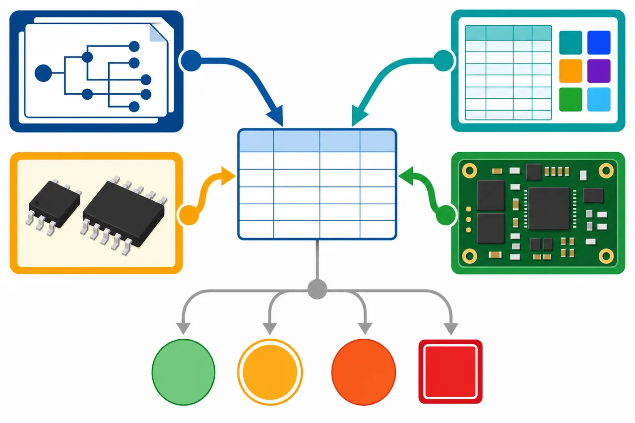
| Claim | Schematic evidence | Physical evidence | Supporting document | Status | Next action |
|---|---|---|---|---|---|
| J? pin 1 is the documented input | Connector symbol and pin/net label | Pin-one marker and recorded viewing side | Connector datasheet or assembly drawing | Confirm, contradict, or unresolved | Cross-probe layout or obtain correct drawing |
| U? is the specified regulator | Reference, value, and connected nets | Package, orientation mark, and readable top mark | BOM plus manufacturer datasheet | Confirm, provisional, contradict, or unresolved | Check approved alternates; never infer from package alone |
| TP? belongs to a named rail | Test-point symbol on that net | Visible designator and accessible pad | Layout/netlist or assembly drawing | Confirm or unresolved | Use synchronized design data before any powered test |
This is an original general-use article worksheet, not a customer record, certification form, or substitute for controlled engineering documentation. Save screenshots or document page references when permitted. Record contradictions instead of overwriting them: a mismatch is often the most useful evidence in the row.
Match Reference Designators, Values, Packages, and Pin 1
A reference designator is the first bridge, not the final answer. Cadence describes it as a cross-reference among the BOM, schematic, board, and assembly. Treat four attributes separately:
- Identity: Does the same reference appear in the schematic, BOM, assembly data, and board view?
- Value or part number: Does the BOM specify the value and exact manufacturer part number? A schematic may show only a generic value or functional label.
- Package: Does the package drawing in the manufacturer datasheet agree with the footprint and observed body dimensions? Similar packages can contain very different devices.
- Orientation: Do the datasheet’s pin-one convention, assembly rotation, footprint numbering, and physical package mark agree?
Do not use the usual prefix list as proof. “R” suggests a resistor role, but it does not establish resistance, tolerance, power rating, technology, or whether that location is populated. A top mark may be abbreviated, reused across vendors, or supplemented by a lot/date code. Confirm it against the BOM and the correct manufacturer’s marking documentation when available.
Dense boards may omit or displace small silkscreen designators. Use the assembly drawing or synchronized EDA cross-probing rather than assigning the nearest label by eye. KiCad, for example, supports bidirectional selection between a schematic symbol or pin and the corresponding PCB footprint or pad when the project files are synchronized.
Verify Connectors, Net Labels, Power Rails, and Ground References
Connector mistakes often begin with viewpoint. A datasheet may show the mating face, terminal side, PCB footprint view, or a section drawing. Before writing “pin 1 is on the left,” record:
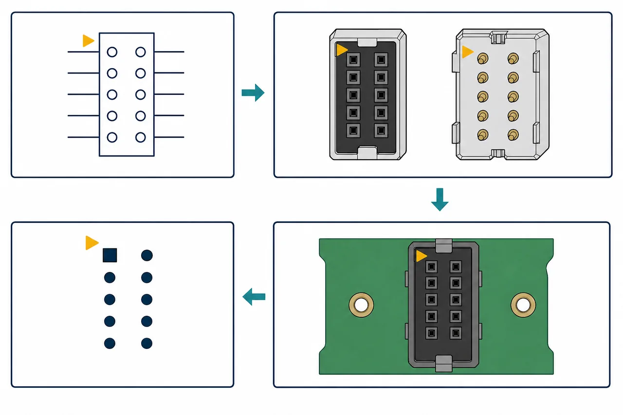
- the document and drawing figure;
- the viewing side;
- the pin-one or polarity marker;
- whether the connector is a plug or receptacle;
- the physical feature used as the reference.
Next, follow net labels rather than page geometry. Two separated symbols with the same controlled net name may be electrically connected without a line drawn between them. Hierarchical sheets can rename or scope signals, so verify the label at each sheet boundary. Likewise, symbols such as chassis ground, protective earth, analog ground, power ground, and digital ground are not automatically interchangeable. Confirm their documented relationship before using one as a measurement reference.
For a power rail, record its source, protection path, switching or regulation stage, return reference, and accessible test point. Do not infer current capacity from trace appearance alone; copper thickness, internal planes, vias, temperature limits, and design requirements are not all visible on an assembled board.
Use Visual Tracing and Meter Measurements Without Overclaiming
Visual tracing is most reliable for exposed outer-layer copper, pads, vias, and clearly labeled test points. It becomes incomplete around inner layers, planes, BGAs, vias-in-pad, conformal coating, shields, buried components, and dense routing. Photograph both sides square-on, preserve orientation, and annotate only what is visible.
For continuity or resistance work, follow the instrument manufacturer’s instructions. Fluke’s continuity guidance calls for a de-energized circuit and notes that the component should be isolated from other circuit paths. Its resistance guidance explains that in-circuit readings can be affected by parallel components and that a capacitor must be discharged before resistance measurement.
| Observation | Supported statement | Unsupported leap |
|---|---|---|
| Visible copper runs from pad A to via B | An outer-layer segment is visibly connected | The via reaches a particular hidden pad or every branch of a net |
| Continuity mode beeps between two de-energized points | The meter detected a path below its configured threshold under those conditions | The points are a dedicated short, the entire documented net is correct, or the circuit will work |
| Resistance is lower than the schematic component value | The in-circuit equivalent resistance between the probes is lower | The component is necessarily wrong; parallel paths can lower the reading |
| Diode mode conducts in one direction | The measured network showed asymmetric behavior at the meter’s test conditions | A specific semiconductor has been identified without isolation and datasheet comparison |
Do not use continuity or resistance mode on a powered circuit. Disconnect sources and verify the test conditions appropriate to the equipment. Batteries and capacitors can preserve energy after an external supply is removed. If you cannot establish an acceptably safe state, stop.
Classify and Resolve Schematic-to-Board Mismatches
A difference is not automatically a defect. Give it a disposition based on evidence:
| Mismatch class | Typical evidence to seek | Disposition |
|---|---|---|
| Revision mismatch | Board identifier, schematic title block, release record | Obtain the matching document set before continuing |
| DNI or configurable option | BOM population flag, assembly variant, option table | Confirm intended variant; do not call an empty footprint a defect |
| Approved alternate | Manufacturer part number, approved-vendor list, change record, compatible datasheet | Verify package, pinout, ratings, and approval scope |
| Documented rework | Rework instruction, marked drawing, engineering change | Compare the physical change to its authorization |
| Damage or unauthorized change | Inspection evidence, production record, traceable test result | Escalate for engineering or quality review; do not modify from appearance alone |
| Ambiguous evidence | Unreadable marking, hidden routing, missing drawing, conflicting documents | Record as unresolved and obtain better evidence |
“Resolve” does not always mean repair the board. It may mean correcting a document, confirming a build option, requesting source design data, or assigning an engineering review. Do not remove, replace, jumper, or power a component merely because it differs from one schematic copy.
Worked Example: Cross-Check One Power-Input Section
This is a source-grounded workflow demonstration, not a report of measurements on a particular board. Arduino’s official UNO R3 hardware page provides downloadable schematics and CAD files, and the official schematic identifies functional blocks including the USB interface, power input and regulation, microcontrollers, headers, LEDs, reset circuitry, and test points. Those public files make the UNO R3 useful for demonstrating document navigation without inventing a customer project.
- Lock the revision. Record “UNO R3” and the revision information from the official schematic title block. Do not substitute files for another UNO version.
- Select one boundary. Choose the power-input block and one documented connector. Avoid claiming that the example covers the entire board.
- Create rows before conclusions. Add the connector, protection elements, regulator, relevant capacitors, power nets, and accessible test points shown in the official files.
- Cross-check attributes. For each row, compare the schematic reference and net names with the CAD/assembly view. Use the official component datasheet for package and pin numbering when the exact manufacturer part is established.
- Record physical observations separately. If you have an actual UNO R3, note visible designators and orientation markers. Do not copy an observation from a product photograph into a claim about your board.
- Stop at the evidence boundary. Without a controlled physical inspection or measurement, the example proves how to navigate the official documents; it does not prove the condition or connectivity of any reader’s board.
The lesson is transferable: a traceable worked example begins with a known revision and controlled files, not with a plausible-looking circuit invented for the article.
Decide When the Evidence Is Sufficient—and When to Stop
| State | Meaning | Next action |
|---|---|---|
| Confirmed | Independent, applicable sources agree and no material contradiction remains | Record the sources and proceed within the verified scope |
| Provisionally supported | Evidence points to one conclusion but a key source or inaccessible feature remains | State the missing evidence; do not present the claim as final |
| Contradicted | Applicable evidence directly disagrees | Check revision and variant, then escalate for controlled disposition |
| Unresolved | Evidence is missing, ambiguous, unsafe to obtain, or mutually inconsistent | Stop and request the correct files, safer access, or qualified support |
Stop when the board revision is unknown, connector viewpoint cannot be established, component identity remains ambiguous, internal routing is essential but unavailable, documentation conflicts, or the next test would expose you to unknown voltage or stored energy. A careful “unresolved” is more useful than a confident guess.
PCB Schematic Cross-Check Checklist
Original general-use article checklist. It is not a certification record and must be adapted to the board, organization, and safety requirements.
Download the PCB Schematic Cross-Check Evidence Worksheet (PDF). This original blank planning worksheet records board/document identity, safety boundaries, claim-level evidence, mismatch dispositions, and stop decisions. It cites its public basis and is not a customer record, test report, certification, release approval, safety procedure, or proof that a board is correct.
- Record the complete board and assembly identifiers exactly as observed.
- Confirm the schematic, BOM, assembly data, and layout belong to the same revision or variant.
- Choose one functional block and define its boundary.
- Create one evidence-map row per component, connector, or net claim.
- Match reference designator, value/part number, package, and orientation separately.
- Record connector viewing side and pin-one reference.
- Trace named nets across sheets and distinguish ground/reference domains.
- Use visible copper only for visible-segment claims.
- For unpowered measurements, confirm isolation, discharged energy, meter mode, threshold, and possible parallel paths.
- Classify each mismatch and attach the evidence needed for disposition.
- Mark every conclusion confirmed, provisional, contradicted, or unresolved.
- Stop when documentation, visibility, authority, or safety is insufficient.
Frequently Asked Questions
Can I identify every PCB component from the schematic?
No. A schematic can provide a reference, value, or functional part number, but the physical identity also depends on the matching BOM, package, assembly option, manufacturer marking, and board revision. Missing or ambiguous evidence should remain unresolved.
Why does the schematic look nothing like the physical PCB?
The schematic arranges symbols to communicate logical connectivity. The PCB places footprints and routes copper under physical, electrical, mechanical, and manufacturing constraints. Compare references and nets, not page position.
Does the nearest silkscreen label always belong to that component?
No. Dense placement can force labels away from footprints, and labels may be missing or covered. Confirm with an assembly drawing, PCB source, or EDA cross-probing.
Does a continuity beep prove two points are on the same schematic net?
It proves only that the meter detected a path below its continuity threshold under the test conditions. Parallel components, planes, semiconductor paths, or other branches may produce that path. Use the layout or netlist when available.
Can I measure continuity while the board is powered?
No. Continuity and resistance modes are intended for de-energized circuits. Disconnect sources and address stored energy according to suitable safety procedures and the instrument manual. If you cannot establish a safe state, stop.
What if the BOM and fitted component differ?
Check the board revision, assembly variant, DNI status, approved alternates, and engineering-change records. Do not assume either an assembly error or an acceptable substitution until applicable records and datasheets support the disposition.
How do I verify pin 1 on a connector?
Use the connector manufacturer’s drawing and record its viewpoint, mating side, terminal side, and pin-one feature. Cross-check that information against the PCB footprint and assembly drawing; never assume left-to-right numbering.
Can I trace all nets visually on a multilayer PCB?
No. Inner layers, planes, buried or blind vias, BGAs, shielding, conformal coating, and pads under packages can hide connectivity. Source layout data, a verified netlist, or specialized inspection may be required.
What should I do when the board revision is missing?
Record the available identifiers and compare only features that can be independently established. Treat revision-dependent conclusions as unresolved and request controlled documentation before modification or powered testing.
Is cross-checking the same as reverse engineering a PCB?
No. Cross-checking tests correspondence between an existing document set and a physical assembly. Reverse engineering attempts to derive missing design information and may require far more imaging, measurement, and analysis, especially for multilayer boards.
Need a PCB Design or Assembly Review?
If your cross-check ends with missing production files, an unresolved BOM/assembly question, or a design that needs manufacturability review, prepare the controlled schematic, PCB files or Gerbers, drill data, BOM, CPL/pick-and-place data, assembly notes, board revision, quantity, and the exact questions you need answered. PCBtry describes PCB design, fabrication, sourcing, and assembly support on its website. Submit the relevant files and request a written scope; do not rely on screenshots or an unmatched schematic alone.
Related PCBtry guides:
- How to Read a Circuit Diagram Schematic for symbols, nets, and signal flow.
- How to Read a PCB for physical layout and component-reading fundamentals.
- How to Trace a PCB Circuit for repair-oriented tracing and continuity checks.
Sources and Applicability
- KiCad PCB Editor documentation — official description of net highlighting and schematic/PCB cross-probing; applicable when synchronized KiCad source files are available.
- Cadence: Component Reference Designators — design-document coordination guidance.
- Fluke continuity testing guide — instrument guidance for de-energized continuity testing.
- Fluke resistance measurement guide — explains discharge and parallel-path limitations in resistance measurement.
- Arduino UNO R3 official hardware page and official UNO R3 schematic — public design documents used only to demonstrate the cross-check method; no physical test result is claimed.
- PCBtry design and handoff guide — current site statement used to scope the CTA and requested file package.
Standards, company procedures, product datasheets, and safety requirements applicable to your board take precedence over this general guide.



0 Comments