




The PCB cleaning process is a controlled manufacturing sequence used to remove particles, oils, oxides, process chemistry, flux and soluble residues at the stages where they would interfere with imaging, plating, soldering, coating or long-term electrical reliability. It is not one universal wash: a bare copper panel before dry-film lamination has a different soil, material risk and acceptance need from an assembled board after soldering.
The correct process begins by identifying the residue and the downstream requirement, then qualifying compatible wash, rinse and drying conditions and verifying the result. PCBtry can review fabrication/assembly data, flux and coating requirements, cleanliness acceptance notes and test needs. Send Gerber or ODB++, BOM/CPL when applicable, material information and the cleanliness specification to [email protected] for an engineering review and quotation.
What Is the PCB Cleaning Process?
PCB cleaning is a set of surface-preparation and residue-removal operations placed between manufacturing steps. Its purpose is to leave a surface that the next operation can wet, bond, image, plate, solder or coat consistently—without replacing one contaminant with another.
Cleaning can occur before photoresist, after drilling/desmear, between wet-process baths, before surface finish, after soldering, after rework and before conformal coating. Some are bare-board fabrication controls; others apply to PCBA. A process is “clean” only against an agreed requirement: visual appearance alone does not prove low ionic residue, and an average ionic result does not identify every localized contaminant.
How Does the PCB Cleaning Process Work?
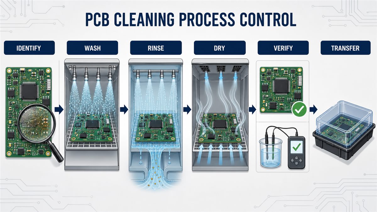
The PCB cleaning process works by identifying the soil, selecting compatible chemistry and mechanical action, removing dissolved contamination with a controlled rinse, drying inaccessible areas and verifying the result before the next manufacturing step.
1. Process-stage and soil identification. Engineers determine what must be removed: fingerprints, oxide, drilling debris, etchant carryover, plating chemistry, solder flux, paste residue, rework contamination or particles. Starting with a familiar solvent instead of the soil can dissolve residue and spread it over a larger area, creating a clean-looking but still contaminated surface.
2. Material and downstream compatibility review. The cleaning route is checked against laminate, solder mask, surface finish, markings, components, adhesives, labels, underfill and the next operation. Excessive chemical strength, temperature, pressure or ultrasonic energy can attack a finish, trap liquid or damage a sensitive assembly. The approved recipe must belong to the actual material set.
3. Pre-clean handling and fixture control. Panels or assemblies are handled by approved edges/fixtures and protected from fingerprints, dust and mixed-metal contamination. Fixtures, baskets and wash equipment must themselves be clean. Poor handling can add oils immediately after a surface has been prepared.
4. Washing and soil release. Aqueous, semi-aqueous, solvent, spray, immersion, vapor or controlled manual methods apply chemistry, time, temperature and mechanical energy to detach and dissolve the target soil. The useful control is the qualified process window, not the name of the machine. Low-clearance components, holes and dense areas need sufficient fluid access.
5. Rinsing and contaminant removal. The rinse carries dissolved soil and cleaning-agent residue away from the product. If the rinse is exhausted, poorly exchanged or unable to reach shadowed areas, contamination can redeposit. This is why “the flux dissolved” is not the same as “the board is clean.” Water quality, rinse stages and drag-out control are part of the manufacturing process.
6. Drying. Free liquid and moisture trapped under components, in holes or around fixtures must be removed without overheating materials. Incomplete drying can interfere with coating adhesion, promote corrosion or produce misleading electrical results. Drying is a validated stage, not idle time after washing.
7. Inspection and cleanliness verification. Visual inspection finds stains, white residue, water marks and particles. Process monitoring and ionic/localized analysis address contamination that eyes cannot see. The test method, extraction area, sampling and limit must be agreed for the product; no single result proves every form of cleanliness.
8. Protection and controlled transfer. Clean product is moved to the next process in clean packaging or controlled handling. Long exposure, bare-hand contact or a dirty carrier can undo the cleaning result before solder mask, finish, coating or final assembly.
| Stage | Main control | Failure signal | Evidence to request |
|---|---|---|---|
| Soil identification | Residue source and chemistry | Smearing, sticky film or repeated cleaning | Material/flux/process identification |
| Wash | Qualified chemistry, time, energy and loading | Remaining residue or material attack | Approved process recipe and monitoring record |
| Rinse | Water/solvent quality and exchange | White film, streaks or redeposition | Rinse-quality and maintenance record |
| Dry | Moisture removal from shadow areas | Water marks, trapped moisture or coating defect | Qualified drying cycle and inspection |
| Verify | Method tied to product risk | Visual pass but electrical/coating failure | Visual, ionic or localized analysis result as specified |
Which Cleaning Methods Are Used for PCB Manufacturing?
Method selection depends on the soil, product geometry, material compatibility, production volume and required evidence. No method is automatically best for every PCB or PCBA.
| Method | Typical fit | Strong point | Qualification concern |
|---|---|---|---|
| Aqueous spray/batch | Water-compatible fluxes and production washing | Wash-rinse-dry can be integrated | Water quality, shadow areas and complete drying |
| Semi-aqueous | Soils needing organic cleaning followed by water rinse | Useful solvency plus rinse removal | Compatibility and rinse completeness |
| Engineered solvent/vapor | Compatible soils and low-clearance assemblies | Penetration and rapid drying can be strong | Material, environmental, equipment and safety qualification |
| Ultrasonic/immersion | Complex geometry when product permits | Fluid reaches immersed surfaces | Cavitation, trapped liquid and component compatibility |
| Controlled manual/local | Prototype, repair or localized rework | Targeted and flexible | Operator variation, smearing and incomplete rinse/dry |
| Mechanical/chemical surface preparation | Bare copper before imaging or bonding | Removes oxide/soil and establishes surface condition | Surface damage, nonuniformity and immediate recontamination |
A cleaning-equipment name does not establish process capability. Ask what soil/product combination has been qualified, how bath/rinse condition is monitored and what happens when loading or component shadowing changes.
How Do Fabrication and PCBA Cleaning Differ?
Bare-board fabrication cleaning prepares exposed material for another chemical or bonding step; PCBA cleaning removes soldering and handling residues around components after assembly. The objects, access paths and failure mechanisms differ.
In fabrication, surface preparation affects dry-film adhesion, plating initiation, etch uniformity and surface finish. The next process may occur immediately, so controlled transfer matters. In PCBA, residues can sit under low-standoff components, beside fine-pitch terminations or beneath coating. Component compatibility and drying become central.
Do not use a PCBA flux-removal recipe as a universal bare-copper preparation step, or treat a bare-board rinse specification as proof that a populated assembly is clean. For the assembly-specific acceptance side, review PCBA cleanliness and defect prevention.
What Are the Main PCB Cleaning Challenges?
The main challenges are matching the chemistry to the residue, reaching hidden surfaces, preventing redeposition, protecting materials and proving dryness/cleanliness at the locations that matter.
- Unknown soil: “residue” may be flux, cleaner, hard-water deposit, oxide, adhesive or mixed contamination.
- Shadowing: low-clearance parts, connectors and dense arrays restrict wash and rinse exchange.
- Redeposition: a dirty brush, wipe, bath or final rinse can spread dissolved soil.
- Material sensitivity: markings, plastics, adhesives, finishes and coatings may react differently.
- Trapped moisture: hidden liquid can remain after the visible surface looks dry.
- Sampling blind spots: a bulk cleanliness result can miss a localized high-risk area.
Design also affects cleanability. Component stand-off, spacing, connector orientation, drainage and fixture access should be reviewed before production when cleaning is required.
How Does Cleaning Affect Reliability and Coating Adhesion?
Cleaning affects reliability by controlling residues that can attract moisture, contribute to leakage/corrosion or block adhesion between the PCB and the next material. It also affects solderability, bond strength and cosmetic quality.
A residue can be electrically quiet in a dry inspection room yet become conductive after absorbing moisture. Conversely, aggressive cleaning can damage a surface or leave a new film. Before conformal coating, even a nominally benign residue can form a weak boundary layer that causes dewetting, bubbles or delamination.
Reliability therefore depends on the complete sequence: compatible wash, sufficient rinse, complete dry, verified result and protected transfer. Cleaning cannot compensate for an incompatible flux/coating system or poor product design.
What Tests Verify PCB Cleanliness?
Use a test plan that combines visible condition with the contamination risk. Each method answers a different question.
| Evidence | What it shows | What it cannot prove alone |
|---|---|---|
| Visual inspection | Stains, particles, white residue, water marks and obvious damage | Invisible ionic or organic residue |
| Process monitoring | Wash/rinse/dry conditions stayed within the qualified window | Every local surface is clean |
| ROSE/ionic extraction | Average soluble ionic contamination under the defined extraction | Residue identity or localized distribution |
| Ion chromatography or localized analysis | Specific ionic species or selected-area contamination | All nonionic films unless the method targets them |
| Coating/wetting or adhesion verification | Downstream surface performance for the qualified system | General electrical cleanliness outside the test |
State the test method, product area, extraction conditions, sampling frequency and acceptance criteria in the purchase documentation. “IPC clean” without a specific applicable requirement and result is not actionable evidence.
What Drives PCB Cleaning Cost and Lead Time?
Cost and lead time depend on the required method, batch/inline loading, chemistry and rinse management, drying time, fixture needs, material qualification, sampling and analytical testing. A product that is hard to drain or has low-clearance components may need more process development than a visually similar open board.
Prototype schedules can also include cleaning trials and coating/adhesion confirmation. Ask the supplier to separate routine production cleaning from one-time qualification and special cleanliness testing. Do not accept a universal lead time before the product, flux and acceptance plan are known.
How Do You Qualify a PCB Cleaning Process and Supplier?
Qualify the process against your exact material, soil and downstream requirement—not a generic statement that the factory has a washing machine.
- Identify every cleaning stage and the soil removed there.
- Confirm material, component, finish, marking and coating compatibility.
- Ask how wash chemistry, concentration/condition, loading and equipment maintenance are controlled.
- Ask how rinse quality and drag-out/redeposition are monitored.
- Confirm how hidden areas are dried and how dryness is validated.
- Define visual, ionic, localized or downstream adhesion evidence and sampling.
- Require change control if flux, cleaner, rinse system, laminate, solder mask or coating changes.
A supplier should be able to explain the failure mechanism behind each control and return a test plan tied to the product. Broader PCBA quality-control methods should complement—not replace—cleanliness verification.
PCB Cleaning Process FAQ
Is PCB cleaning always required after soldering?
No. The decision depends on the flux system, product environment, coating/bonding needs and cleanliness requirement. “No-clean” is a process classification, not proof that every residue is acceptable in every application.
Can visual inspection prove a PCB is clean?
It can detect visible residue and damage but not all ionic or organic contamination. Use additional evidence when reliability or downstream adhesion requires it.
Why does white residue appear after cleaning?
Possible causes include partially removed flux, contaminated rinse, hard-water minerals, cleaner residue or redeposition. Identify the material before changing chemistry.
Is isopropyl alcohol a universal PCB cleaner?
No. Its effectiveness depends on the soil and concentration, and dissolving residue without removing it can spread contamination. Production processes must qualify the complete wash-rinse-dry sequence.
Can ultrasonic cleaning damage a PCB assembly?
It can be suitable for some products, but components, solder joints, cavities and trapped-liquid risks must be evaluated. Use only a qualified process for the actual assembly.
Why is drying part of the cleaning process?
Moisture can remain under components and in holes after the visible surface dries. Trapped moisture can affect electrical testing, corrosion risk and coating adhesion.
What files are needed for a PCB cleaning quotation?
Send Gerber/ODB++, BOM and CPL for assemblies, assembly drawings, material/finish data, flux and coating information, quantities and the cleanliness/test specification.
What cleanliness evidence should a buyer request?
Request the agreed visual criteria, process-monitoring record and any specified ionic/localized/adhesion result with method, sample and acceptance limit identified.
Send the Right Data for a PCB Cleaning Review
Send Gerber or ODB++, BOM/CPL where applicable, assembly drawings, laminate/solder-mask/surface-finish details, flux and coating systems, quantities, cleaning restrictions and the required test/acceptance method. Email [email protected] and request a cleaning-process compatibility review, verification plan and quotation before production release.



0 Comments