




The flex PCB assembly process mounts and solders components onto a flexible circuit while the circuit is held flat, registered and mechanically protected. The SMT sequence resembles rigid-board assembly, but the process controls are different: thin polyimide can absorb moisture, move on a printer, deform under placement force and concentrate strain near pads, stiffeners and bend transitions.
A production-ready build therefore starts before solder paste printing. PCBtry reviews the bare-flex construction, Gerber data, BOM, CPL, assembly drawings, panel/carrier concept, formed condition and test requirements together. Send these files for a DFM and quotation review so the assembly route is agreed before tooling and material release.
What Is Different About Flex PCB Assembly?
Flex assembly is primarily a mechanical-control problem added to a normal soldering process. A rigid PCB naturally presents a stable plane to the stencil, placement machine and conveyor; a flex circuit needs a panel, carrier, vacuum support or other fixture to create that plane without damaging the intended bend region.
Stiffeners support connectors or component zones but also create a change in local stiffness. If a pad or solder joint sits too close to that transition, handling or final forming can place strain where the copper and joint are least tolerant. Assembly DFM must therefore review both the flat manufacturing state and the installed state.
What Files and Decisions Are Needed Before Assembly?
The assembler needs more than a BOM and centroid file because those files do not describe how the flex should be supported, bent or tested.
- Gerber, ODB++ or IPC-2581 data and the approved flex stack-up.
- NC drill and outline/profile data with panel rails and tooling features.
- BOM with manufacturer part numbers, substitutions and moisture/handling notes.
- CPL/centroid data with units, origin, rotation and side definition.
- Assembly drawings showing polarity, connector orientation and stiffener locations.
- Flat-state and formed-state drawings, bend zones, bend direction and keep-outs.
- Stencil requirements, accepted solder alloy and component thermal limits.
- Inspection class, electrical/functional test plan and acceptance samples.
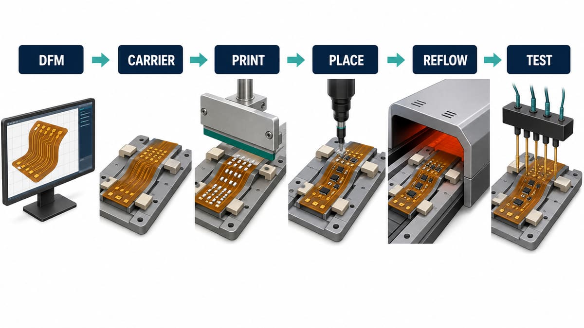
How Does the Flex PCB Assembly Process Work?
The process should keep one traceable relationship from released files to the final tested flex assembly. Each step has a flex-specific control and a stop condition.
Step 1: Joint DFM and data validation. Engineering reconciles BOM, CPL, Gerber and drawings, then checks pad geometry, component clearances, stiffener transitions, bend keep-outs, panel support and test access. A mismatch in origin or connector orientation must be resolved before programming.
Step 2: Incoming inspection and conditioning decision. The lot is checked for identity, flatness, surface condition, packaging history and visible damage. Baking or other conditioning follows the actual flex material, storage exposure, finish, component restrictions and controlled procedure—not an internet-wide temperature recipe.
Step 3: Carrier and tooling setup. The flex panel is located and supported so stencil contact and placement coordinates remain stable. Pins, vacuum, adhesive or covers must avoid functional copper and bend regions and must release without peeling coverlay or stressing parts.
Step 4: Solder paste printing and SPI. A verified stencil deposits paste while the carrier holds the pads in one plane. SPI checks volume, area, height and offset where required; a shifted panel can make an otherwise correct stencil print unusable.
Step 5: Component placement. Pick-and-place programs use the approved CPL convention, feeder setup and polarity data. Nozzle selection and placement force must suit the component and supported flex zone; an unsupported area can deflect and create offset or incomplete seating.
Step 6: Pre-reflow verification. Operators or automated inspection confirm critical polarity, registration, missing parts and disturbed paste before heat fixes the defect into the assembly.
Step 7: Profiled reflow. The thermal profile is verified for the solder paste, component limits, flex construction, carrier thermal mass and load. The goal is adequate soldering without trapping moisture, overheating adhesives or creating excessive temperature difference across the panel.
Step 8: AOI, X-ray and secondary assembly. AOI checks visible joints and placement; X-ray is used where hidden terminations or risk justify it. Connectors, through-hole parts, stiffeners or reinforcement operations follow the approved sequence so later heat and force do not damage completed joints.
Step 9: De-tooling and handling inspection. The assembly is removed from the carrier using defined support points. Inspect for coverlay lifting, creases, pad damage and component movement; careless peeling can create damage after all SMT checks passed.
Step 10: Electrical, functional and final testing. Testing confirms the product requirements in the state specified by the drawing. If the product operates while formed or moves repeatedly, a flat continuity test alone may not reveal strain-sensitive failures.
How Should Carriers, Stencils and Stiffeners Be Planned?
The carrier, stencil and flex panel form one tooling system. Support must exist directly beneath printing and placement areas, but locating features should not force the flex into a distorted position. Tooling also needs a repeatable way to load, unload and identify the panel orientation.
| Item | Engineering control | Failure if missed | Evidence to request |
|---|---|---|---|
| Carrier datum | Matches panel and machine origin | Systematic paste/placement offset | Approved tooling drawing and first-article result |
| Local support | Supports pads without loading bend zones | Print variation or flex deformation | Carrier contact map |
| Stencil aperture | Matches pad, component and paste needs | Bridges, opens or solder-volume imbalance | Stencil review plus SPI data where specified |
| Stiffener transition | Keeps joints and traces away from strain concentration | Copper or solder fatigue during forming | Stack-up and formed-state drawing review |
| Release method | Removes flex without peel or point load | Coverlay lift, crease or cracked joint | Work instruction and handling inspection |
How Is the Reflow Profile Controlled?
Use a measured profile on the actual product/carrier combination. A carrier can change heating rate and temperature uniformity, while flex construction and copper distribution change local thermal response. Thermocouple locations should represent the thermally light and heavy areas and critical components.
Supplier datasheets define solder-paste and component boundaries; the flex material and adhesive system add their own constraints. A successful profile produces acceptable joints without blistering, delamination, coverlay lift or damage to temperature-sensitive parts. Record the approved recipe and revalidate it when the carrier, panel, paste, component loading or oven changes materially.
What Flex Assembly Defects Should Engineers Watch?
| Failure | Possible cause | Production impact | Prevention/checkpoint |
|---|---|---|---|
| Paste or placement offset | Panel shifts or bows on carrier | Bridges, opens, tombstoning | Datum check, carrier support, SPI/first article |
| Blister or delamination | Moisture/process incompatibility or excessive thermal stress | Latent interconnect and coverlay damage | Exposure record, qualified conditioning and measured profile |
| Cracked trace near stiffener | Sharp stiffness transition or forced forming | Intermittent/open circuit in use | Formed-state DFM and strain-aware test |
| Solder wicking or weak joint | Pad/stencil imbalance or unsuitable process sequence | Reduced joint volume and reliability | Stencil review and joint inspection |
| Damage during de-tooling | Peel force or unsupported component zone | Late scrap after assembly | Defined removal method and post-release inspection |
What Inspection and Testing Prove Assembly Quality?
Inspection must match the defect mechanism. SPI measures paste before placement; AOI checks visible placement and solder features; X-ray supports hidden-joint review; electrical or in-circuit testing checks nets and components; functional testing checks behavior. None alone proves dynamic flex life.
For static flex, test in the agreed final shape when forming could stress conductors or joints. For dynamic flex, define the motion, bend geometry, cycles, monitoring method and failure criterion with the product engineer. A generic “flex test” without these inputs is not an acceptance plan.
How Do You Choose a Flex PCB Assembly Supplier?
Choose the supplier that can explain the proposed support, thermal and verification route for your specific construction. Ask to see the DFM questions, carrier concept, first-article controls, profile-validation method, hidden-joint inspection scope, de-tooling method and test boundary.
- Can fabrication and assembly engineers review stiffeners, coverlay openings and component pads together?
- Who owns BOM/CPL/assembly-drawing discrepancies?
- How will the carrier locate and support the flexible panel?
- Which inspections are automatic, sampled or project-specific?
- How is formed-state or dynamic testing defined and recorded?
- What evidence accompanies prototype approval and repeat production?
Frequently Asked Questions
Can flex PCBs use standard SMT components?
Often yes, if land patterns, support, thermal limits and mechanical use are suitable. Heavy or mechanically loaded parts may need a stiffened zone or a different interconnect strategy.
Does every flex PCB need baking before assembly?
No universal rule fits every material and exposure history. Use the flex supplier’s guidance, packaging/storage record and controlled assembly procedure; excessive or incompatible baking can also create risk.
Why is a carrier required?
A carrier presents a stable, flat and repeatable plane to printing, placement, reflow transport and inspection. Its locating and release design matter as much as its stiffness.
Can components be placed in the bend area?
That is usually a high-risk choice because components, pads and solder joints resist bending and concentrate strain. Confirm the formed geometry and keep-out rules with fabrication and assembly engineering.
Is AOI enough for flex assembly?
AOI is useful for visible placement and solder features but cannot inspect every hidden joint or prove electrical function and bend life. Combine methods according to package and product risk.
When is X-ray inspection needed?
X-ray is useful for bottom-terminated or otherwise hidden solder joints when visual inspection cannot answer the acceptance question. Scope and sampling should be agreed before production.
How should assembled flex circuits be packaged?
Packaging should prevent sharp folds, uncontrolled bending, abrasion, contamination and load on components or connectors. The shipment form should match the approved drawing or handling instruction.
What files are needed for a quotation?
Send Gerber or ODB++, NC drill data, BOM, CPL, assembly and formed-state drawings, stack-up, quantities, panel preference, solder/test requirements and acceptance criteria.
Prepare a Flex Assembly Package for Engineering Review
Send PCBtry the fabrication data, BOM, CPL, assembly drawing, flex stack-up, stiffener details, formed-state drawing, quantities and test requirements. The review can then identify carrier, stencil, thermal, inspection and handling risks before prototype tooling or volume production is released.



0 Comments