




The flexible PCB testing process should verify the released geometry, visible construction, electrical continuity and isolation, and the circuit’s behavior in its intended mechanical state. A flat electrical test can catch opens and shorts at shipment, but it cannot by itself prove that a flex circuit will survive forming once or bending repeatedly in service.
The test plan must therefore start from product duty. PCBtry reviews Gerber or ODB++, netlist, stack-up, drawings, bend zones, static or dynamic use, quantities and acceptance requirements before fabrication. Send those inputs for an engineering review and quotation so inspection evidence matches the actual risk.
What Is a Flexible PCB Testing Process?
It is a staged verification route that compares a flex circuit with its design data and intended use. It normally combines incoming/material controls, dimensional and visual inspection, electrical testing, targeted construction evidence and any product-specific forming, bend or environmental validation.
The key is not the number of tests. Each method must answer a defined question: “Are the nets correct now?”, “Is the internal construction acceptable?”, or “Does resistance remain stable during the specified motion?” Mixing these questions produces certificates that look complete but leave the main field risk untested.
What Must Be Defined Before Testing Starts?
Define how the flex moves, where it is constrained and what failure means before choosing equipment. A dynamic cable that cycles in a hinge needs a different plan from a flex tail formed once inside a housing.
- Released Gerber/ODB++ data, drill files and netlist.
- Stack-up, material, copper, coverlay and stiffener drawing.
- Static-form or dynamic-flex classification and installed shape.
- Bend axis, direction, radius, travel, frequency and environmental conditions.
- Critical circuits and whether resistance must be monitored during motion.
- Sample size, cycles or exposure duration, checkpoints and failure criteria.
- Applicable acceptance standard and customer-specific drawing notes.
How Does the Flexible PCB Testing Process Work?
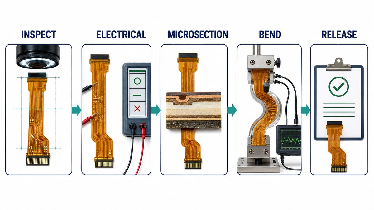
A useful factory flow moves from low-cost, non-destructive checks to evidence that targets the project’s main reliability risks.
Step 1: Data and test-plan review. Engineering reconciles layer data, netlist, drawing tolerances, bend zones, critical nets and acceptance requirements. Missing motion inputs are raised before a generic bend test is invented.
Step 2: Material and process traceability. Verify the approved construction, lot identity and required process records. A test result cannot validate a different material build.
Step 3: Dimensional and visual inspection. Check outline, connector fingers, holes, stiffeners, coverlay openings, surface condition, registration and visible damage. Pay special attention to edges and rigid-to-flex or stiffener transitions where stress can concentrate.
Step 4: Electrical continuity and isolation. Test the finished netlist with suitable fixture or flying probes. Support the circuit so probe force does not crease the flex; record whether testing uses customer-supplied net data or data derived from artwork.
Step 5: Construction verification. When risk or acceptance requirements justify it, coupons or representative microsections evaluate plated holes, layer interfaces and material construction. This is destructive sampling, so the location and representation matter.
Step 6: Static forming or dynamic bend test. Form the circuit in the specified direction and fixture, or cycle it through the defined motion. Avoid arbitrary folding: fixture geometry must reproduce the product use without adding unrelated clamp damage.
Step 7: In-situ and post-test measurements. Monitor critical-net resistance or function during motion when intermittent opens matter, then repeat visual/electrical checks after the exposure. A circuit may reconnect when returned flat, hiding a bend-induced crack.
Step 8: Review and release. Compare results with written criteria, link failures to panel/lot data, contain affected material and issue the agreed inspection evidence. Pass/fail cannot be decided after testing by selecting whichever observation looks favorable.
Which Test Method Finds Which Flex PCB Risk?
| Method | Answers | Does not prove | Buyer evidence |
|---|---|---|---|
| Visual/AOI and dimensional inspection | Visible pattern, openings, outline and workmanship | Hidden interfaces or future bend life | Inspection report and approved drawing |
| Electrical continuity/isolation | Net connectivity at test conditions | Internal geometry or latent fatigue | Netlist basis and test result |
| Microsection | Representative internal construction | Every circuit or dynamic lifetime | Coupon location and cross-section record |
| Static-form check | Fit and connection after one defined forming event | Repeated-motion endurance | Fixture/shape and post-form readings |
| Dynamic bend cycling | Behavior during a defined repeated motion | Other radii, axes, loads or environments | Setup, cycles, monitoring and failure rule |
| Functional/environmental test | Product behavior under specified combined conditions | Root cause without failure analysis | Procedure, conditions and logged result |
How Should Static and Dynamic Bend Tests Differ?
A static flex is installed or formed and then remains largely stationary; validate the formed geometry, strain at transitions and electrical condition after assembly. A dynamic flex repeats motion, so the plan must define the entire duty cycle and monitor for transient as well as permanent changes.
“Bend it 1,000 times” is not a reproducible specification without radius, travel, neutral position, speed, clamp locations, conductor orientation, temperature and failure threshold. The customer owns the use case; the manufacturer should confirm the fixture can reproduce it and state what is measured.
What Failures Require More Than a Continuity Check?
| Failure signal | Possible cause | Why flat continuity can miss it | Useful next evidence |
|---|---|---|---|
| Intermittent open while moving | Fatigue crack in copper or transition | Crack faces reconnect at rest | In-situ resistance during defined motion |
| Resistance gradually increases | Developing conductor or plated-interface damage | Still below simple pass/open threshold | Trend log plus failure analysis |
| Coverlay lift or edge tear | Geometry, adhesion or clamp stress | Net remains electrically intact initially | Visual inspection in formed state |
| Post-reflow connection failure | Marginal via/interface exposed by thermal stress | Bare-board test occurred before assembly heat | Post-stress electrical test and microsection |
| Connector-area failure | Stiffener alignment, insertion or local strain | Unmated fixture does not reproduce load | Mated functional/form-state test |
How Are Test Fixtures Designed Without Damaging the Flex?
The fixture should locate the circuit repeatably, support probe/contact zones and reproduce the intended bend without pinching traces or loading component/stiffener transitions. Clamp surfaces, edge radii and cable routing must be documented so the fixture does not become the failure source.
For electrical fixtures, verify contact force and test-point accessibility. For bend rigs, photograph or dimension the setup and identify the monitored nets. A supplier report should make it possible to distinguish a product failure from a loose probe, connector or clamp.
How Do You Choose a Flexible PCB Testing Supplier?
Choose a supplier that asks for the mechanical use case before quoting a “flex test.” Review its ability to relate data, fabrication records, electrical test, coupons, fixtures and failure analysis rather than relying on one generic certificate.
- What netlist source is used, and are all circuits tested or sampled?
- Which visual/dimensional features are controlled at bend and stiffener transitions?
- What evidence supports plated-hole or internal-layer acceptance?
- Can the fixture reproduce the actual formed or moving state?
- Is resistance/function monitored during motion or only afterward?
- How are failure criteria, lot containment and retest documented?
Frequently Asked Questions
Is electrical testing enough for a flexible PCB?
It verifies nets at the test condition but does not prove construction or future flex life. Add visual, construction or bend evidence according to the failure risk.
Does every flex circuit need dynamic bend testing?
No. A circuit formed once may need a static formed-state check, while repeated-motion products need an application-specific endurance plan.
Should resistance be measured during bending?
Yes when intermittent opens or small resistance changes are important. A cracked conductor may reconnect when the sample returns flat.
Can the manufacturer choose the bend radius?
The product design must define the intended geometry and duty. The manufacturer can review manufacturability and fixture feasibility but should not invent the use condition.
What does a microsection show?
It shows representative internal geometry and interfaces at the sectioned location. Because it is destructive and sampled, agree on coupon/location and acceptance purpose.
When should testing occur?
Use stage-appropriate checks after fabrication and, where assembly heat or forming changes risk, repeat relevant electrical or functional tests afterward.
How many bend cycles are required?
There is no universal number. Define it from expected service duty, safety margin, test acceleration rationale and applicable product/industry requirements.
What files are needed for a test quotation?
Send fabrication data, netlist, stack-up, drawings, bend definition, critical nets, sample quantity, environmental conditions, monitoring needs and acceptance criteria.
Define the Evidence Before Ordering
Send PCBtry the Gerber or ODB++ package, netlist, stack-up, flex drawings, static/dynamic duty, bend geometry, quantities and acceptance requirements. Engineering can then align fabrication controls, electrical testing, coupons and any bend-validation plan with the actual application before quotation and production release.



0 Comments