




Flexible PCBs replace the glass-reinforced core of a rigid board with a thin polyimide-based construction that can fold, route through tight spaces, or move repeatedly when the design is qualified for dynamic flexing. They are used in cameras, medical devices, wearables, automotive modules, compact sensors, and cable-replacement assemblies. The manufacturing difference is not merely a softer substrate: every imaging, drilling, plating, coverlay, and profiling operation must account for a panel that expands, contracts, wrinkles, and carries mechanical strain into its copper.
A useful manufacturing review therefore starts with the bend application, stack-up, copper type, coverlay openings, stiffener locations, and acceptance evidence—not with price alone. Send your Gerber data, drill and outline files, stack-up, bend drawing, surface finish, and inspection requirements through PCBTRY’s engineering contact for a DFM review and quotation.

What Is the Flexible PCB Manufacturing Process?
The flexible PCB manufacturing process converts copper-clad polyimide into a circuit that remains electrically continuous in its intended installed shape. The sequence resembles rigid-board fabrication, but registration, adhesive flow, copper grain direction, coverlay alignment, and edge condition have a much larger influence on field reliability.
The first purchasing decision is whether the circuit is installation-flex—bent mainly during assembly—or dynamic-flex—expected to move during use. The same outline can require different copper, conductor routing, bend geometry, and qualification testing depending on that answer.
How Does the Flexible PCB Manufacturing Process Work?
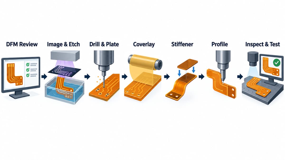
The process below is one connected control chain. A defect found at final test may have originated in data preparation, panel movement, drilling debris, plating, or coverlay lamination, so each lot needs traceable in-process evidence.
1. Engineering review and DFM analysis. CAM engineers reconcile Gerbers, drill data, outline, stack-up, impedance notes, bend zones, stiffeners, and connector geometry. They look for vias or sharp trace corners in the bend area, abrupt width changes, unsupported pads, ambiguous coverlay openings, and mismatched dimensions. If the installed bend and flex duty are not defined, a manufacturer can build a board that passes continuity yet fails after assembly.
2. Stack-up and material preparation. Copper-clad polyimide, coverlay, bonding films, stiffeners, and pressure-sensitive adhesives are selected as one material system. Thin panels must be cleaned and handled without creases or contamination. Moisture, incorrect material orientation, or uncontrolled dimensional change can shift registration later, so lot identity and material certificates should remain linked to the traveler.
3. Imaging and copper etching. The conductor image is aligned, exposed, developed, and etched. Because the substrate does not hold dimensions like FR-4, compensation and panel registration matter. Over-etching reduces trace width; under-etching leaves copper that can narrow spacing or create shorts. AOI before the circuit is covered gives the best chance to catch conductor defects.
4. Drilling, cleaning, and plating. Mechanical or laser processes form holes according to feature size and construction. Smear or debris must be removed before hole-wall metallization. Registration error can leave an annular ring vulnerable; weak or discontinuous plating can survive a room-temperature test and open when the flex is bent or thermally cycled.
5. Coverlay preparation and lamination. Openings are cut for pads, contacts, and test points, then the polyimide coverlay is aligned and laminated. The manufacturer controls opening position, pressure, temperature, and adhesive movement. Window offset can cover a pad; excess adhesive can intrude into the opening; trapped air, wrinkles, or incomplete bonding can become delamination paths.
6. Stiffener and adhesive bonding. FR-4, polyimide, or metal stiffeners may reinforce connector, component, or mounting regions. The critical detail is the edge transition: a poorly located or lifted stiffener creates a stress concentration exactly where the circuit leaves the rigid support. Drawings should define material, thickness, side, position, adhesive, and tolerance rather than simply state “add stiffener.”
7. Surface finish, legend, and final profile. Exposed copper receives the specified finish, identification is applied where permitted, and the flex outline is routed, punched, or laser cut. The selected method must protect narrow necks and internal corners. Burrs, carbonized residue, micro-tears, or a notch at a bend edge can initiate cracking even when the electrical pattern is correct.
8. Inspection and testing. Final release normally combines visual and dimensional inspection with electrical continuity/isolation testing. Requirements may also call for AOI records, microsections, impedance coupons, ionic cleanliness, adhesion checks, or a defined bend/flex test. The test method, sample size, conditioning, bend radius, stroke, and cycles must be agreed before production; “flex tested” without conditions is not reproducible evidence.
What Materials Are Used in Flexible PCB Manufacturing?
Material choice should follow the mechanical duty, electrical performance, assembly temperature, thickness target, and environment. “Polyimide flex” is not a complete stack-up specification.
| Material element | What it controls | RFQ evidence to request |
|---|---|---|
| Copper-clad polyimide | Base thickness, flexibility, dimensional behavior, conductor fatigue | Material family, copper type and thickness, dielectric construction |
| Adhesive or adhesiveless construction | Total thickness, thermal behavior, bond interfaces | Stack-up drawing and approved material substitution rule |
| Polyimide coverlay | Conductor protection and pad-access geometry | Film/adhesive construction, window dimensions and registration tolerance |
| Stiffener | Connector support, assembly flatness, local thickness | Material, thickness, side, adhesive and positional tolerance |
| Surface finish | Solderability, contact interface, storage and assembly compatibility | Finish type, exposed-pad scope and acceptance requirement |
How Should the Flex Stack-Up and Bend Region Be Designed?
The bend region should be treated as a mechanical structure, not spare routing space. Route conductors smoothly through the bend, avoid sudden copper-density changes, keep plated holes and component terminations outside the stressed region when possible, and define whether the bend is static or repeated. Staggering conductors and avoiding sharp corners reduces local strain concentration.
Do not copy a generic bend-radius rule without identifying total thickness, copper construction, layer count, bend angle, and flex cycles. Ask the fabricator to return a controlled stack-up and mark the no-via, no-component, and stiffener-transition zones on the manufacturing drawing.
What Are the Key Manufacturing Challenges?
- Dimensional stability: thin polyimide changes size during wet processing and heat, challenging drill, image, and coverlay registration.
- Coverlay windows: cut size, alignment, and adhesive flow jointly determine usable pad area.
- Via reliability: drilling quality, desmear, plating, and mechanical strain interact at the hole wall.
- Transition stress: stiffener edges, connector exits, and rigid-to-flex changes concentrate strain.
- Final profiling: a small edge nick in a flexing zone may matter more than a cosmetic mark elsewhere.
How Does Design Affect Flexible PCB Reliability?
Manufacturing cannot fully compensate for copper routed across a hinge at a sharp angle, an unsupported pad pulled by a cable, or a stiffener that ends at the maximum bend point. Reliability improves when the drawing communicates the installed shape and the designer separates electrical features from mechanical transitions.
A useful DFM package includes the flat outline, folded-state drawing, bend direction and angle, bend region, expected flex duty, connector mating thickness, stiffener details, critical dimensions, and test requirement. That lets engineering review the actual load path before tooling is released.
What Tests Ensure Flexible PCB Quality?
| Check | Question it answers | Evidence to keep |
|---|---|---|
| AOI and visual inspection | Are conductors, coverlay, pads, and edges free from observable defects? | Inspection criteria and defect record |
| Electrical test | Does the netlist pass continuity and isolation? | Test method and lot result |
| Dimensional inspection | Do outline, openings, stiffeners, and connector features fit? | FAI or dimensional report for critical features |
| Microsection/coupon | Is the plated structure built as specified? | Coupon identity and report when required |
| Application-specific flex test | Does the circuit survive the defined motion? | Fixture, radius, angle, cycles, conditioning and failure criterion |
How Long Does Flexible PCB Manufacturing Take?
Lead time depends on material availability, layer count, via structure, coverlay tooling, stiffeners, controlled impedance, special profiling, coupon requirements, and qualification testing. A prototype with stocked materials and standard inspection is a different scheduling problem from a multilayer dynamic-flex build with custom fixtures. For a useful commitment, freeze the data package and ask the supplier to separate engineering review, material procurement, fabrication, special testing, and shipment in the schedule.
How Do You Choose a Flexible PCB Manufacturer?
Choose on evidence relevant to your construction. Ask the supplier to explain how it compensates panel movement, inspects conductors before coverlay, controls coverlay/stiffener registration, profiles delicate outlines, and links final tests to the lot. A useful quote should list material construction, exclusions, test scope, and open engineering questions rather than hide them behind “standard flex process.”
- Can the supplier return a controlled stack-up and bend-region DFM comments?
- Will material substitutions require approval?
- Which inspections are 100% and which are sampled?
- What report identifies critical dimensions and test conditions?
- How are nonconforming lots contained and traced?
Frequently Asked Questions
What files are needed for a flexible PCB quotation?
Provide Gerbers, NC drill data, outline/profile data, stack-up, fabrication drawing, bend drawing, stiffener details, surface finish, quantity, and inspection requirements. Add netlist and impedance information when applicable.
Is every flexible PCB suitable for repeated bending?
No. A circuit designed only to bend during installation may not tolerate continuous motion. Dynamic flex requires an explicit mechanical duty and matching design, material, and test plan.
Why does coverlay alignment matter?
A shifted opening can reduce pad access or expose a conductor that should be protected. Adhesive flow can further change the usable opening, so window geometry and lamination control must be reviewed together.
What causes cracked traces near a stiffener?
Common contributors are an abrupt stiffness transition, tight bend location, sharp conductor geometry, edge damage, or repeated motion outside the design assumptions. Failure analysis should examine both copper and the mechanical stack.
Can solder mask replace coverlay?
Some constructions use flexible photoimageable coatings, but they are not an automatic equivalent for every bend duty or environment. Specify the protective material and obtain supplier confirmation for the application.
How is a flexible PCB electrically tested?
The finished netlist is tested for continuity and isolation using suitable fixtures or flying probes. This confirms connectivity at test time but does not by itself prove dynamic-flex life.
Should bend testing be required on every order?
Only when the application and acceptance plan justify it. Define the fixture, radius, angle, rate, cycles, conditioning, sample count, and failure criterion so results are comparable.
What should a first-article report cover?
Prioritize connector geometry, outline, coverlay openings, stiffener position/thickness, critical stack-up features, and agreed electrical or coupon results. Tailor the report to the design risks rather than requesting a generic certificate.
Send a Manufacturing-Ready Flex RFQ
A strong flex RFQ tells the factory how the circuit will move and how success will be judged. Send the complete data package through PCBTRY’s contact page and request a DFM response that identifies material, bend, coverlay, stiffener, profiling, and test assumptions before production.



0 Comments