




The LED PCB assembly process converts a fabricated board and controlled LED/components into a tested lighting assembly. It includes engineering review, material and bin verification, solder-paste printing, component placement, reflow or through-hole soldering, inspection, electrical and optical testing, thermal verification, and release. LED assemblies need more than a standard SMT flow because polarity, package marking, color/brightness bin, moisture sensitivity, thermal-pad quality, and heat removal can change visible performance and lifetime.
Before quotation, send the Gerber or ODB++ data, BOM with exact LED part numbers and approved bins, centroid file, assembly drawings, polarity references, substrate/thermal requirements, and test limits. PCBtry can review these inputs through the contact page before prototype or production release.

What Makes LED PCB Assembly Different?
An LED is electrically directional and optically graded, while higher-power packages also depend on a low-resistance thermal path. A board can pass continuity yet fail its brightness, color, thermal or reliability requirement. The process must therefore connect material traceability and solder-joint control with optical and thermal acceptance.
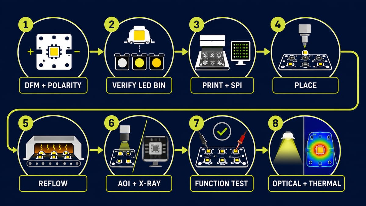
How Does the LED PCB Assembly Process Work?
The complete route keeps the same product revision, component lot and test specification connected from DFM through shipment.
1. Engineering and DFM Review
Engineering checks the footprint, polarity convention, board material, copper/thermal structure, stencil intent, panelization, fiducials, clearance, test points and mechanical interface. A reversed footprint or missing thermal requirement cannot be corrected reliably by line inspection.
2. BOM, LED Bin and Lot Verification
Receiving verifies manufacturer part number, package, forward-voltage/color/brightness bin requirements, quantity, date/lot information and approved substitutions. Mixing uncontrolled bins can create visible nonuniformity even when every LED functions.
3. Storage and Material Preparation
LED packages and solder materials are handled according to their documented storage, moisture and preparation requirements. The correct action comes from the component and material documentation; unnecessary or incorrect baking can damage packaging or finishes.
4. Solder-Paste Printing
The stencil deposits paste onto each pad and thermal land. SPI, when required by the quality plan, checks deposit position and volume. Imbalanced deposits can rotate or tombstone small LEDs; an unsuitable thermal-pad aperture can contribute to voiding or package float.
5. Pick-and-Place
The machine places each LED from a controlled feeder with verified rotation and centroid data. First-article inspection should compare package marking, board marking, assembly drawing and programmed orientation. One wrong library rotation can reverse an entire panel.
6. Reflow Soldering
The populated panel follows a profiled thermal cycle compatible with the solder paste, LED package and board thermal mass. The factory should profile the actual build where risk warrants it. Excess heat can damage packaging; inadequate heat or wetting can leave weak or open joints.
7. Through-Hole or Secondary Assembly
Connectors, larger LEDs or mixed-technology parts may require selective, wave or controlled manual soldering. Polarity, seating height, lead stress and heat exposure remain controlled. Mechanical loading on LED leads or lenses can create damage that visual inspection misses.
8. AOI, Visual and X-Ray Inspection
AOI checks presence, position, polarity and visible solder features. X-ray is useful when the critical joint or thermal pad is hidden, but acceptance must be tied to an agreed quality plan rather than an arbitrary image. Inspection findings require disposition and feedback.
9. Electrical and Functional Test
Testing verifies shorts/opens, driver behavior, LED string operation and required functions using controlled voltage/current. A simple light-on check does not fully prove current balance, intermittent joints, communication behavior or optical uniformity.
10. Optical, Thermal and Final Release
Projects may require brightness, color, uniformity or thermal measurements under defined conditions. Final release confirms revision, traceability, inspection/test status, workmanship, labeling and packaging. Exact limits must come from the customer specification.
Which Inputs Must Be Controlled Before Production?
| Input | Required decision | Failure if unclear |
| LED MPN and bin | Exact device and allowed optical/electrical range | Color, brightness or voltage mismatch |
| Polarity data | Datasheet marking, footprint pin map and CPL rotation | Dark LED or damaged string |
| Thermal design | Package land, board construction, interface and heatsink path | High junction temperature |
| Stencil/paste | Aperture intent and qualified solder system | Bridges, opens, float or void risk |
| Test specification | Electrical, optical and thermal conditions/limits | Functional boards that still miss product performance |
How Should LED Polarity Be Verified?
Use the component datasheet and verified footprint pin map as the primary references. Package dots, chamfers, lead length and PCB silkscreen conventions vary; no single visual shortcut is universal.
- Record anode/cathode or pin-one mapping in the assembly drawing.
- Confirm centroid rotation against one physical first article.
- Use clear board markings that do not conflict with the datasheet.
- Test a controlled first unit before releasing the lot.
How Does Thermal Design Affect Assembly Quality?
The heat path runs from LED junction through package, solder joint, PCB, interface material and heatsink or enclosure. A metal-core board alone does not guarantee a good path. Voids, poor contact, warped assemblies, incorrect interface thickness or inadequate mounting can increase thermal resistance.
Review the board and mechanical assembly together. Define how thermal performance will be verified and under what ambient, current and mounting condition; otherwise temperature measurements from different setups are not comparable.
Which Defects Need Which Evidence?
| Symptom | Possible causes | Evidence |
| One LED dark | Reversal, open joint, wrong part, damaged LED | AOI, polarity record, continuity and controlled diode/function test |
| String dark | Driver/power fault, one open device, connector error | Rail/current measurements and node-by-node isolation |
| Uneven brightness/color | Mixed bin, current variation, thermal gradient | Lot traceability, current data and optical test |
| Early thermal failure | Joint crack/void, poor interface, inadequate heat path | X-ray/section where appropriate and defined thermal measurement |
| LED shifted after reflow | Paste imbalance, placement or wetting asymmetry | SPI, placement and reflow records |
What Tests Should an LED PCBA Receive?
The test plan should match product risk and acceptance needs. Combine inspection with electrical and performance evidence.
| Test | What it checks | Limitation |
| SPI/AOI | Paste and visible placement/solder features | Cannot prove optical output or all hidden joints |
| X-ray | Hidden joint/thermal-land structure | Needs defined acceptance and interpretation |
| Continuity/ICT | Opens, shorts and selected component nodes | Does not prove end-use light performance |
| Functional test | Driver, strings, dimming and controls | Test coverage depends on fixture/program |
| Optical/thermal test | Specified light and temperature behavior | Requires controlled conditions and limits |
How Does Design Affect Reliability?
Reliability begins with correct current regulation, thermal path, footprint, copper distribution, mechanical support and protection against the actual environment. Provide test points and separate strings so failures can be isolated. Avoid placing mechanically stressed connectors where cable forces bend the LED board.
How Long Does LED PCB Assembly Take?
Lead time depends on component availability and bin control, board construction, stencil/fixture preparation, first-article approval, inspection/test scope, quantity and rework risk. Prototype and production dates should be quoted only after the complete files and material status are reviewed.
How Should You Choose an LED PCB Assembly Supplier?
Ask for project-specific controls rather than generic SMT claims. Review how the supplier verifies polarity and bin, profiles the actual build, handles moisture-sensitive parts, inspects hidden pads, performs functional/optical/thermal tests, controls substitutions and traces component lots.
LED PCBA RFQ Checklist
- Gerber/ODB++, drill files, stackup and fabrication notes
- BOM with exact LED MPN, bin requirements and substitution policy
- CPL with units, origin, side and rotation convention
- Assembly drawing with polarity and special handling notes
- Board/heatsink/interface mechanical information
- Electrical drive conditions and current limits
- Optical, thermal and functional test conditions and acceptance limits
- Programming, labeling, traceability and packaging requirements
Frequently Asked Questions
Can LEDs be assembled with a normal SMT line?
Many SMD LEDs can, provided the line uses the verified package data, stencil, placement, thermal profile and inspection plan. The exact process depends on the LED and board construction.
Why does an LED remain dark after assembly?
Check polarity, solder continuity, driver output, current limiting and device damage in that order. A clean-looking joint does not prove electrical connection.
Does AOI detect reversed LEDs?
AOI can when the package marking, reference image and inspection program support reliable recognition. First-article and functional verification still provide important independent evidence.
Why are LED bins important?
Bins group devices by specified optical or electrical characteristics. Mixing outside the approved range can create visible color or brightness differences and affect driver margins.
Is aluminum PCB always required?
No. Substrate choice depends on power, heat path, isolation, mechanics, cost and validation needs. Evaluate the complete thermal system rather than choosing by material name alone.
How are hidden thermal-pad joints checked?
X-ray or other qualified process evidence may be used where risk and acceptance requirements justify it. The test method and limits should be agreed before production.
What files are needed for LED PCBA quotation?
Provide fabrication files, BOM, CPL, assembly drawing, polarity/bin notes, mechanical/thermal data and test requirements. Use one controlled revision across every file.
Should every board receive optical testing?
That depends on product risk, specification and test economics. Define whether sampling or 100% testing is required and the controlled conditions used to judge results.
Request an LED PCB Assembly Review
Send PCBtry the controlled fabrication package, BOM, CPL, polarity/bin requirements, thermal interface data and test limits through the contact page. Engineering review can resolve footprint, polarity, thermal and test gaps before the first production panel is assembled.



0 Comments