
Blog
OSP Process in PCB: Surface Preparation, Coating and Solderability Checks
See how the OSP process in PCB manufacturing controls copper preparation, coating, inspection, handling and assembly solderability.



See how the OSP process in PCB manufacturing controls copper preparation, coating, inspection, handling and assembly solderability.

Follow the metal core PCB manufacturing process from stackup and dielectric bonding through imaging, machining, insulation tests and thermal checks.
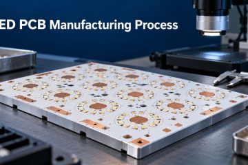
Learn how LED PCBs are engineered and fabricated, how thermal stack-up choices affect reliability, and which inspection and testing evidence to request.
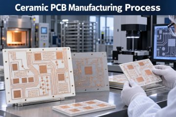
See how ceramic PCB substrate, metallization route, circuit formation, profiling, inspection and reliability testing are selected and controlled.
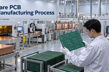
See how bare PCBs move from CAM review through imaging, lamination, drilling, plating, finishing, inspection and electrical testing.
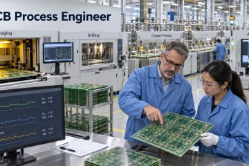
Learn how a PCB process engineer controls fabrication, qualification, yield, troubleshooting, changes and supplier evidence.
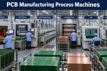
Understand PCB manufacturing machines by process function, controlled output, utilities, qualification, maintenance and supplier evidence.
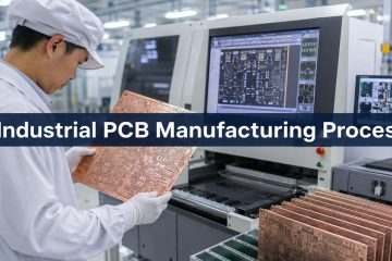
Follow the industrial PCB manufacturing process from DFM and material control through imaging, lamination, plating, finishing, inspection, testing and supplier release.
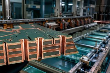
See how heavy copper PCBs move from DFM and stack-up review through plating, etching, lamination, drilling and release testing—with buyer checks at each stage.
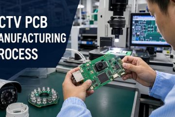
Follow the CCTV PCB manufacturing process from DFM and bare-board fabrication through SMT assembly, programming, image testing and final release.
If you have any enquiry about quotation or cooperation, please feel free to email us at [email protected] or use the following enquiry form. Oursales representative will contact you within 24 hours. Thank you for your interest in our products.