




An RF PCB is a printed circuit board built to carry radio-frequency signals with controlled impedance, low loss, stable grounding, and predictable electromagnetic behavior. In RF work, the PCB is not just a carrier for components. The board material, copper geometry, stackup, via transition, solder mask, connector launch, and ground return all become part of the circuit.
If you are asking “What is RF PCB?” the short answer is this: it is a PCB designed for signals that are sensitive to frequency-dependent loss, reflection, coupling, and impedance mismatch. These boards are common in Wi-Fi, Bluetooth, GPS, radar, RF front-end modules, antennas, 5G equipment, IoT devices, industrial wireless systems, and satellite communication hardware.
A low-speed board can often tolerate small layout mistakes. An RF board usually cannot. A trace that looks harmless in CAD may behave like a filter, radiator, antenna stub, or impedance discontinuity once the frequency gets high enough. That is why RF PCB design and manufacturing need to be handled with tighter material, stackup, layout, and process control.
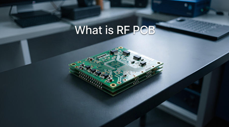
What Is an RF PCB?
An RF PCB is a circuit board designed for radio-frequency signal transmission where trace geometry, dielectric material, and grounding directly affect electrical performance.
In practical engineering work, a board starts to become “RF-sensitive” when the signal wavelength becomes short enough that the PCB trace can no longer be treated as a simple wire. Many wireless products work from hundreds of MHz to several GHz, and at those frequencies, a few millimeters of routing can change matching, phase, loss, or radiation behavior.
Most RF systems are designed around a controlled impedance, commonly $50\ \Omega$. That does not mean every copper trace on the board is $50\ \Omega$. It means the RF signal path, such as an antenna feed, filter input, amplifier output, or connector launch, must be designed and manufactured to match the intended impedance as closely as practical.
A good RF PCB keeps the signal path short, the return path clean, the reference plane solid, and the dielectric properties predictable. A poor RF PCB may still pass a basic continuity test, but fail during real RF testing because of high return loss, low output power, poor receiver sensitivity, unexpected harmonics, or unstable performance between production lots.
Why RF PCBs Are Different from Standard PCBs
RF PCBs are different because copper traces behave like transmission lines instead of simple connections.
On a standard PCB, the main concerns are often connectivity, current capacity, spacing, solderability, and assembly quality. On an RF circuit board, the shape of the copper is part of the electrical design. Trace width, spacing to ground, dielectric thickness, copper thickness, solder mask coverage, via position, and even copper roughness can change how the signal travels.
This is why RF boards often fail in ways that are not obvious from visual inspection. The board may look clean. The components may be placed correctly. The circuit may power up. But the antenna match may be wrong, the insertion loss may be too high, or the RF power may drop after assembly because the layout or material was not controlled tightly enough.
| Parameter | Standard PCB | RF PCB | Engineering Impact |
|---|---|---|---|
| Trace behavior | Mostly treated as connection paths | Designed as transmission lines | Affects impedance, phase, and signal reflection |
| Material choice | FR-4 is often acceptable | Low-loss laminate or hybrid stackup may be required | Controls dielectric loss and frequency stability |
| Ground reference | Important for noise and EMC | Critical for return current and field control | Poor grounding can increase radiation and coupling |
| Manufacturing tolerance | Moderate variation may be acceptable | Tighter process control is usually needed | Trace width and dielectric thickness affect impedance |
| Testing focus | Open/short, AOI, functional test | Impedance, return loss, insertion loss, RF performance | Basic electrical tests cannot verify full RF behavior |
How an RF PCB Works
An RF PCB works by guiding electromagnetic energy along a controlled path while reducing reflection, loss, and unwanted coupling.
At RF frequencies, the signal is not only “inside” the copper trace. The useful energy is carried by the electromagnetic field around the trace and its reference plane. That is why the dielectric constant, board thickness, trace width, ground clearance, and nearby copper all matter.
The most common RF transmission structures are microstrip, stripline, coplanar waveguide, and grounded coplanar waveguide. Each one controls the relationship between the signal conductor and its return path. If that relationship changes suddenly, the signal sees an impedance step. Part of the energy continues forward, and part of it reflects back.
In a real product, those small mismatches can reduce antenna efficiency, shift filter response, lower amplifier output, or create measurement results that do not match simulation. The layout goal is not only to connect RF pins together. The goal is to preserve the intended impedance and field structure from one RF block to the next.
Main Types of RF PCB Transmission Structures
The right RF PCB structure depends on frequency, board size, isolation requirements, stackup, available fabrication process, and cost target.
For many compact wireless products, top-layer microstrip or grounded coplanar waveguide is common because it is easy to route, easy to tune, and convenient for antenna or connector access. For higher isolation or multilayer RF routing, stripline may be used because the signal is buried between reference planes.
There is no universal “best” structure. A short Bluetooth antenna feed and a 77 GHz radar board have very different requirements. The safest approach is to choose the structure during stackup planning, not after routing has already started.
| Structure | Typical Application | Relative Cost | Limitation |
|---|---|---|---|
| Microstrip | Antenna feed lines, RF modules, simple wireless products | Low to medium | More exposed to radiation, solder mask, and external influence |
| Stripline | Multilayer RF boards, high-isolation signal paths | Medium to high | Harder to probe, tune, and inspect after fabrication |
| Coplanar waveguide | Compact RF routing and impedance-controlled paths | Medium | Requires careful gap control to nearby copper |
| Grounded coplanar waveguide | RF front-end modules, connector launches, dense wireless boards | Medium | Needs proper via stitching and ground continuity |
| Hybrid RF stackup | RF plus digital, RF plus power, 5G and industrial control boards | Medium to high | Material bonding and lamination control become more complex |
Common RF PCB Materials
RF PCB materials are selected for stable dielectric constant, low loss, controlled thickness, thermal reliability, and repeatable manufacturing behavior.
FR-4 can work in some low-frequency or cost-sensitive RF designs, especially when the RF trace is short and the performance margin is wide. But as frequency rises, FR-4 becomes less predictable because dielectric constant and loss can vary more than dedicated RF laminates. For demanding RF designs, engineers usually look at PTFE-based laminates, hydrocarbon ceramic materials, low-loss high-speed laminates, or hybrid stackups.
The key material properties are dielectric constant, loss tangent, thickness tolerance, copper type, thermal expansion, moisture absorption, and compatibility with the PCB factory’s lamination process. A material may look good in a datasheet but still create production problems if the stackup is not practical or if the fabrication process is not controlled well.
| Material Type | Suitable Scenario | Relative Cost | Limitation |
|---|---|---|---|
| FR-4 | Low-cost RF, short traces, lower-frequency wireless designs | Low | Higher loss and less stable dielectric behavior at high frequency |
| Low-loss high-speed laminate | RF-digital mixed boards, communication modules, controlled impedance boards | Medium | Material choice must match frequency and loss target |
| PTFE-based RF laminate | Microwave, radar, satellite, high-performance RF paths | High | Fabrication is more demanding than standard FR-4 |
| Hydrocarbon ceramic laminate | Stable RF performance, antenna boards, high-frequency modules | Medium to high | Stackup and availability should be confirmed early |
| Hybrid RF material | RF layer combined with FR-4 digital or power layers | Medium to high | Lamination, CTE mismatch, and registration need attention |
RF PCB Stackup and Impedance Control
RF PCB stackup should be fixed before layout because impedance depends on trace width, dielectric height, copper thickness, and reference plane position.
A common mistake is routing the RF section first and asking the factory to “make it $50\ \Omega$” later. That is risky. If the dielectric thickness or copper thickness changes, the calculated trace width changes too. On small RF boards, even a small stackup change can force layout rework.
For an RF PCB, the stackup should define the RF material, core thickness, prepreg type, copper weight, plating allowance, solder mask condition, reference planes, controlled-impedance layers, and acceptable tolerance. When possible, impedance should be calculated with a field solver instead of relying only on rough formulas.
Engineers should also decide whether the RF traces will be covered by solder mask. Solder mask changes the dielectric environment above a microstrip trace. In some designs this change is small enough to accept. In tighter designs, RF traces may need to be kept free of solder mask, or the impedance model must include the mask effect.
RF PCB Design Rules Engineers Actually Care About
Good RF PCB design is mostly about keeping the signal path controlled and the return path uninterrupted.
Keep RF traces short and direct. Avoid unnecessary stubs. Do not route RF lines across splits in the reference plane. Place matching networks close to the RF pin or antenna feed where they are actually useful. Use smooth transitions instead of abrupt geometry changes. Keep noisy digital clocks, switching regulators, and high-current paths away from sensitive RF traces.
Grounding needs more attention than many new RF designers expect. A solid ground plane under the RF path is usually better than broken copper. Via stitching around RF traces, connectors, filters, and shield areas can help control return current and reduce leakage. The spacing and placement of ground vias should be planned, not sprinkled randomly after layout.
Connector launch design is another common source of trouble. A beautiful $50\ \Omega$ trace can still perform poorly if the SMA, U.FL, board-to-board connector, or antenna pad transition is not designed correctly. The pad size, ground clearance, via fence, anti-pad, and layer transition should match the connector recommendation and the actual PCB stackup.
Manufacturing Process for RF PCBs
RF PCB manufacturing requires tighter control of material handling, lamination, etching, drilling, plating, solder mask, and final inspection than many standard PCB builds.
The process usually starts with stackup confirmation. For RF boards, this step is not paperwork. It decides whether the final impedance and loss target are realistic. After that, the factory controls inner-layer imaging, etching compensation, lamination pressure, drilling accuracy, copper plating, solder mask registration, surface finish, and routing tolerance.
Etching control is especially important because trace width directly affects impedance. Over-etching or under-etching can shift RF performance. For plated through holes and via transitions, drill quality and plating reliability matter because poor via structure can increase loss, create discontinuity, or reduce long-term reliability.
Surface finish should be selected with the product requirement in mind. ENIG is widely used because it provides good solderability and flatness, but RF performance, frequency, contact interface, assembly process, and cost should all be considered before final selection.
RF PCB Testing and Quality Control
RF PCB quality control should verify both normal PCB reliability and RF-specific performance risks.
Standard checks include visual inspection, AOI, electrical open/short testing, dimensional inspection, solder mask inspection, and board flatness review. For production and acceptance criteria, common references include IPC-A-600 for bare board acceptability, IPC-6012 for rigid PCB qualification and performance, IPC-A-610 for assembled board workmanship, UL 796 for printed wiring boards, and RoHS compliance where required.
For RF boards, additional checks may include controlled-impedance coupons, time-domain reflectometry testing, insertion loss measurement, return loss measurement, and functional RF testing. Not every RF PCB needs every test. A simple low-cost wireless board and a radar module should not be treated the same way.
The useful question is not “Can the factory make a PCB?” The useful question is “Can the factory hold the stackup, trace geometry, material, and test method that this RF design depends on?”
Advantages and Limitations of RF PCBs
RF PCBs make compact wireless and high-frequency systems possible, but they also bring tighter design rules, higher material sensitivity, and more demanding manufacturing control.
The main advantage is performance integration. RF PCBs allow antennas, filters, amplifiers, mixers, matching networks, sensors, connectors, digital control, and power circuits to fit into a compact product. With the right material and stackup, they can deliver stable impedance, controlled loss, and repeatable RF behavior across prototypes and production.
The limitation is that mistakes are less forgiving. Material substitution, uncontrolled trace width, poor reference planes, careless via transitions, and undocumented stackup changes can all damage RF performance. RF PCB cost is also usually higher than standard FR-4 boards when low-loss materials, tight impedance, advanced stackups, or RF testing are required.
| Factor | Advantage | Limitation | Practical Advice |
|---|---|---|---|
| Signal performance | Supports controlled RF transmission | Sensitive to mismatch and layout changes | Lock stackup before layout |
| Board size | Enables compact wireless products | Dense layouts increase coupling risk | Separate RF, digital, and power sections carefully |
| Material | Low-loss laminates improve performance | Higher cost and more process control | Use RF material only where it is needed if hybrid stackup is suitable |
| Manufacturing | Repeatable boards are possible with the right process | Trace tolerance and lamination variation affect results | Confirm impedance tolerance and test method early |
Where RF PCBs Are Used
RF PCBs are used wherever a product needs to transmit, receive, process, or guide high-frequency signals.
In consumer electronics, RF boards are found in smartphones, wearables, smart speakers, wireless earbuds, cameras, game devices, and smart home products. These designs usually care about compact size, low cost, antenna performance, and stable mass production.
In automotive electronics, RF PCBs are used in radar sensors, keyless entry systems, vehicle communication modules, GPS units, smart cockpit systems, and some ADAS hardware. These applications require strong reliability, thermal performance, vibration resistance, and long product life.
In communication equipment, RF circuit boards are used in 5G infrastructure, RF front ends, base stations, satellite communication, routers, optical modules, and high-speed networking hardware. These projects often need low loss, strict impedance control, high-layer-count boards, and stable material supply.
Industrial and medical devices also use RF boards in wireless sensors, test instruments, imaging equipment, monitoring systems, RFID readers, and remote control modules. In these fields, reliability and noise control often matter as much as pure RF performance.
Common RF PCB Failure Modes
Most RF PCB failures come from impedance discontinuity, material mismatch, poor grounding, assembly variation, or layout details that were not visible in a simple schematic review.
One common problem is weak RF output. The root cause may be excessive insertion loss, wrong trace impedance, bad matching component placement, poor connector launch, or lossy material used beyond its practical range. Another common problem is unstable antenna performance. This often comes from enclosure effects, ground size changes, nearby metal, solder mask influence, or late-stage mechanical changes.
Intermittent RF performance can be even harder to debug. A board may work on the bench but fail after assembly into the housing. In that case, check the antenna environment, cable routing, shield contact, grounding screws, board warpage, connector quality, and assembly pressure points.
| Symptom | Likely Cause | What to Check First |
|---|---|---|
| High return loss | Impedance mismatch or poor matching network | Trace width, stackup, component placement, antenna feed |
| High insertion loss | Lossy material, long route, rough copper, bad via transition | Material datasheet, route length, vias, connector launch |
| Poor antenna range | Bad ground, enclosure effect, antenna detuning | Antenna keepout, ground plane, housing material, nearby metal |
| Lot-to-lot performance drift | Material or process variation | Laminate batch, stackup tolerance, etching control, impedance reports |
| Unexpected radiation | Broken return path or noisy coupling | Ground plane cuts, via stitching, clock routing, power supply noise |
How to Choose the Right RF PCB Solution
The right RF PCB solution should be chosen from frequency, loss budget, impedance requirement, product size, reliability target, and production volume.
Start with the operating frequency and acceptable loss. If the RF path is short and the product has enough margin, a controlled FR-4 design may be acceptable. If the frequency is high, the path is long, or the design needs stable performance over temperature and production lots, a low-loss RF laminate is usually safer.
Next, decide whether the whole board needs RF material or only part of it. Many products use hybrid stackups: RF material for critical RF layers and FR-4 or high-speed material for digital and power sections. This can reduce cost, but it must be reviewed carefully because hybrid lamination adds process complexity.
Also check the assembly environment. RF performance can change after shields, cables, connectors, antennas, and housings are installed. For products with embedded antennas or tight mechanical spaces, PCB design and enclosure design should be reviewed together.
Cost Factors in RF PCB Manufacturing
RF PCB cost is mainly affected by material type, board thickness, layer count, impedance tolerance, copper weight, surface finish, special processing, testing, and order volume.
Material is often the first cost driver. Dedicated RF laminates cost more than standard FR-4, and some materials require longer lead times or more careful processing. Layer count is another major factor. A simple two-layer RF board is very different from a multilayer hybrid RF-digital board with controlled impedance, blind vias, shielding, and tight dimensional requirements.
Testing also affects cost. Controlled-impedance coupons, TDR reports, RF performance checks, and extra inspection steps are valuable when the design needs them, but they should be specified clearly. Over-testing a simple board wastes money. Under-testing a high-frequency board creates risk.
The best way to control RF PCB cost is to define the real performance requirement early. Do not use expensive material just because the board is called “RF.” But do not force FR-4 into a high-frequency design where loss and variation will cost more later in debugging and failed production.
Procurement Checklist Before Ordering RF PCBs
Before ordering RF PCBs, buyers should confirm the stackup, material, impedance, tolerance, testing method, surface finish, and assembly requirements with both the engineer and the manufacturer.
For RF boards, a Gerber package alone is often not enough. The manufacturer should receive the fabrication drawing, stackup requirement, controlled-impedance table, material brand or acceptable alternatives, copper weight, board thickness, surface finish, solder mask requirement, special notes for RF traces, and test requirements.
If material substitution is allowed, define the electrical limits clearly. Do not approve a substitute only by thickness or price. For RF work, dielectric constant, loss tangent, copper type, thickness tolerance, and process compatibility matter.
| Item to Confirm | Why It Matters | Common Mistake |
|---|---|---|
| RF material | Controls loss and dielectric stability | Approving substitutes without checking RF properties |
| Stackup | Defines impedance and manufacturability | Changing dielectric thickness after layout |
| Controlled impedance | Reduces reflection and mismatch | Not specifying tolerance or test coupon requirements |
| Solder mask over RF traces | Can affect microstrip impedance | Leaving mask condition undefined |
| Surface finish | Affects solderability, flatness, and contact interface | Selecting finish only by price |
| Assembly constraints | Shields, antennas, and connectors affect RF behavior | Reviewing bare board only, not final assembled product |
How Thindry Supports RF PCB Projects
Thindry supports RF PCB projects by combining PCB fabrication, component sourcing, PCBA assembly, engineering review, and production control in one workflow.
For RF boards, early review is valuable. Our engineering team can check stackup feasibility, impedance requirements, material selection, manufacturability risks, solder mask notes, surface finish choice, and assembly concerns before the design moves into production. This is especially useful for wireless modules, communication equipment, industrial control boards, automotive electronics, IoT devices, and high-frequency prototypes moving toward volume production.
As a China-based PCB and PCBA manufacturer with global supply capability, Thindry focuses on practical manufacturing support instead of false local claims. We work with customers on prototype builds, engineering validation, BOM optimization, SMT assembly, through-hole assembly, mixed-technology PCBA, and batch production. Quality systems and compliance requirements can be matched according to project needs, including ISO 9001, ISO 13485, IATF 16949, UL certified PCB requirements, and RoHS compliance where applicable.
FAQ About RF PCBs
What is RF PCB in simple words?
An RF PCB is a printed circuit board made for radio-frequency signals. It is used when the board layout, material, grounding, and impedance directly affect signal quality. Unlike a normal PCB trace that may only act like a connection, an RF trace works as a controlled transmission line.
What frequency is considered RF for PCB design?
RF usually refers to radio-frequency signals from kHz ranges up to GHz ranges, but PCB design becomes more sensitive as frequency rises and wavelength becomes shorter. In many practical projects, engineers start applying RF layout rules from hundreds of MHz, especially for antennas, wireless modules, and high-speed RF paths.
Can FR-4 be used for RF PCB?
FR-4 can be used for some low-cost or lower-frequency RF designs, especially when RF traces are short and performance margins are not tight. For higher-frequency, low-loss, or highly repeatable RF products, dedicated RF laminates are usually safer because they offer more stable dielectric properties and lower loss.
Why is $50\ \Omega$ common in RF PCB design?
$50\ \Omega$ is widely used because it provides a practical balance between power handling and signal loss in many RF systems. RF instruments, connectors, antennas, filters, amplifiers, and cables are commonly designed around $50\ \Omega$, so matching the PCB trace to this impedance helps reduce reflection.
What is the difference between RF PCB and high-speed PCB?
An RF PCB focuses on radio-frequency behavior such as impedance matching, insertion loss, return loss, coupling, antenna performance, and electromagnetic fields. A high-speed PCB usually focuses on digital signal integrity, timing, crosstalk, eye diagrams, and power integrity. Some boards need both RF and high-speed design rules.
What materials are best for RF PCB?
The best material depends on frequency, loss target, budget, and manufacturing process. Common choices include low-loss high-speed laminates, PTFE-based RF materials, hydrocarbon ceramic laminates, and hybrid stackups. FR-4 may be acceptable for simple low-frequency RF boards, but it is not ideal for every RF application.
Does solder mask affect RF PCB performance?
Yes, solder mask can affect RF performance, especially on microstrip traces where the electromagnetic field exists partly above the copper. The effect may be small in some designs but important in tighter RF circuits. Engineers should define whether RF traces are covered or exposed and include that condition in impedance modeling.
What causes poor RF PCB performance?
Common causes include wrong material, uncontrolled stackup, impedance mismatch, poor grounding, long RF traces, bad connector launch design, excessive vias, antenna detuning, solder mask variation, and poor isolation from digital or power circuits. Many RF issues come from small layout details that are easy to miss during schematic review.
How do you test an RF PCB?
Basic PCB tests include open/short testing, AOI, dimensional inspection, and visual checks. RF-specific testing may include controlled-impedance testing, TDR measurement, insertion loss, return loss, antenna matching, and functional RF testing with proper instruments. The required test depends on product frequency and performance risk.
Is a two-layer RF PCB acceptable?
A two-layer RF PCB can work for simple designs if it has a clear signal layer, a solid reference ground, controlled trace geometry, and short RF paths. However, dense products, high-isolation circuits, RF-digital mixed systems, and higher-frequency designs often benefit from multilayer stackups with better shielding and routing control.
What should I send to a manufacturer for RF PCB quotation?
Send Gerber files, drill files, fabrication drawing, stackup requirement, material specification, impedance table, board thickness, copper weight, surface finish, solder mask notes, testing requirements, and assembly files if PCBA is needed. For RF designs, stackup and impedance notes are just as important as the copper artwork.
How can I reduce RF PCB cost without hurting performance?
Start by identifying which traces truly need RF-grade material and tight impedance. A hybrid stackup may reduce cost if only part of the board carries critical RF signals. Avoid unnecessary layer count, over-tight tolerances, and excessive testing, but do not remove controls that protect impedance, material stability, or RF performance.
Final Thoughts
An RF PCB is not just a standard circuit board with a wireless chip on it. It is a controlled electromagnetic structure where material, stackup, copper shape, grounding, vias, connectors, and manufacturing tolerance all affect the final signal. The safest design path is to confirm frequency, loss target, impedance, material, stackup, solder mask condition, and test method before layout is locked.
For selection, do not choose the most expensive RF laminate automatically. Choose the material and stackup that match the real frequency, route length, loss budget, reliability requirement, and production volume. For purchasing, make sure your supplier can control the RF details that matter: material traceability, impedance tolerance, etching accuracy, lamination consistency, inspection, and assembly quality.
If you need RF PCB fabrication, high frequency PCB manufacturing, RF circuit board assembly, prototype validation, or volume production support, you can contact our engineering team at [email protected].
If you’re sourcing reliable PCB/PCBA manufacturing — OEM, ODM, prototyping, mass production, or custom engineering solutions — reach out to our engineering team for technical support and a quote at [email protected].



0 Comments