




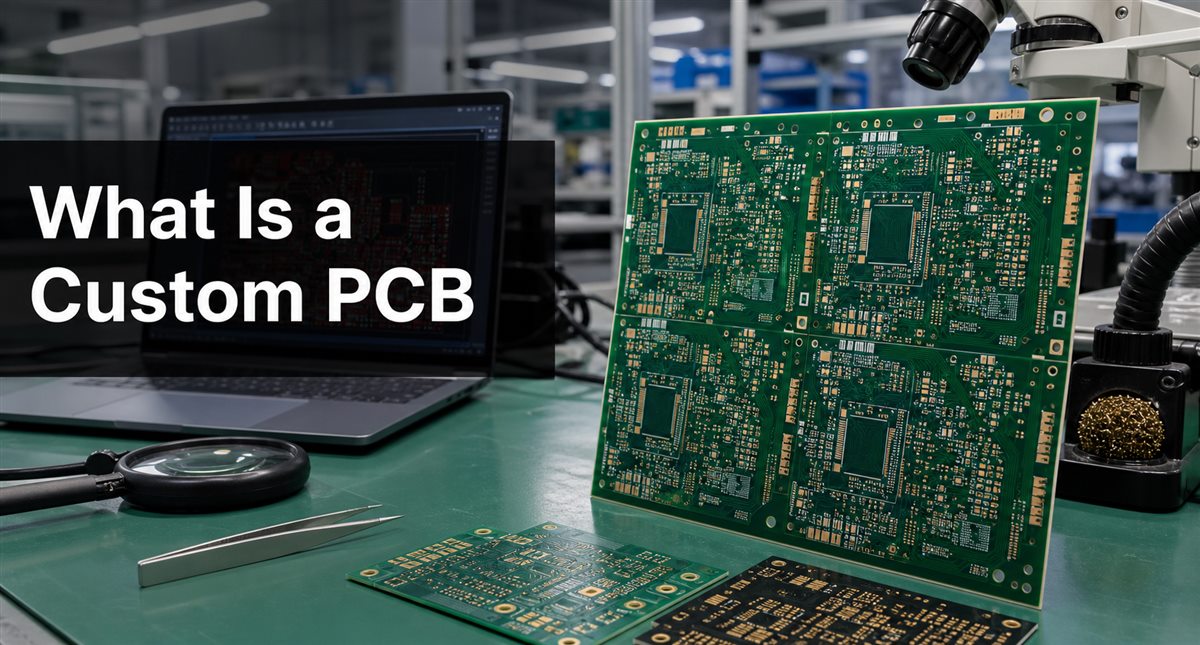
A custom PCB is a printed circuit board designed for a specific electronic product instead of a generic development board or off-the-shelf module. It defines the exact circuit layout, board size, layer stackup, materials, surface finish, holes, solder mask, silkscreen, and manufacturing requirements needed for that product.
For engineers and buyers, the real value of a custom PCB is control. You can make the board fit the enclosure, reduce wiring, support the required current or signal speed, improve assembly consistency, and prepare the product for repeatable production. The trade-off is that the design files, manufacturing notes, and supplier checks must be correct before fabrication starts.
What Makes a PCB Custom?
A PCB becomes custom when its physical and electrical design is created for one product’s circuit, enclosure, performance target, and manufacturing route.
Custom does not only mean a strange board shape or a high layer count. A simple two-layer FR-4 board can still be custom if its copper traces, mounting holes, connector positions, and component footprints are designed for a specific device. The board may be optimized for low cost, compact size, thermal performance, vibration resistance, controlled impedance, or easier assembly.
Common custom details include board outline, layer count, copper weight, via type, solder mask color, silkscreen markings, surface finish, impedance control, material grade, panelization method, test points, and acceptance requirements.
Custom PCB vs Standard PCB Module
A custom PCB is built around your product requirements, while a standard module is built for general reuse across many projects.
| Comparison Point | Custom PCB | Standard Module or Development Board |
| Fit | Matches the enclosure, connector locations, and mechanical limits. | Uses a fixed size and connector arrangement. |
| Electrical design | Routing, copper width, stackup, and grounding can be tuned for the product. | Performance depends on the module design and available pins. |
| Prototype speed | Requires layout, file export, DFM review, and fabrication. | Fast for early proof-of-concept work. |
| Production cost | Often lower at volume because unused circuits, connectors, and wiring can be removed. | May cost more per finished product when extra adapters or wiring are needed. |
| Risk | Design errors can create unusable boards if files are not checked. | Lower layout risk, but less control over long-term supply and fit. |
Many projects start with standard modules and move to a custom PCB after the circuit is proven. That path reduces early engineering risk while giving the final product a cleaner, more repeatable hardware platform.
When Should You Use a Custom PCB?
You should consider a custom PCB when the product needs repeatable manufacturing, a specific mechanical fit, better reliability, or lower unit cost at scale.
A custom board is usually worth the effort when hand wiring becomes hard to inspect, cables create assembly variation, the enclosure has limited space, the circuit carries higher current, the design needs controlled impedance, or the product will be assembled repeatedly. It is also useful when the PCB must support exact connector positions, mounting holes, thermal paths, shielding, or test points.
For a one-off experiment, a breadboard, perfboard, or module may be enough. For a sellable product, field trial, industrial controller, medical device accessory, IoT gateway, power board, or LED product, a custom PCB usually gives better control over quality and production repeatability.
Common Types of Custom PCB
Custom PCBs can be simple or complex depending on the layer structure, material, signal requirements, and application environment.
| Type | Typical Use | What to Check |
| Single-sided PCB | Simple low-cost circuits, LED boards, basic controls. | Jumper needs, trace width, and assembly access. |
| Double-sided PCB | Most common prototypes and compact electronic products. | Via count, grounding, connector placement, and solderability. |
| Multilayer PCB | Dense routing, power integrity, high-speed signals, compact products. | Stackup, impedance, via structure, and lamination capability. |
| Rigid-flex PCB | Folded assemblies, wearables, cameras, compact devices. | Bend radius, stiffener design, copper fatigue, and IPC-2223 guidance. |
| Metal core PCB | LED lighting, power electronics, heat-spreading applications. | Thermal path, dielectric thickness, insulation, and mechanical mounting. |
| HDI PCB | Fine-pitch ICs, smartphones, modules, dense embedded electronics. | Microvias, laser drilling, sequential lamination, and supplier capability. |
What Files Are Needed to Make a Custom PCB?
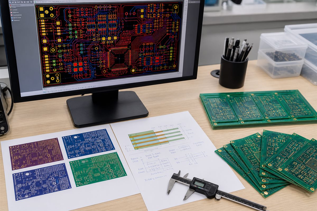
For bare PCB fabrication, the minimum package usually includes Gerber or ODB++ production data, drill files, board outline, stackup notes, and fabrication requirements.
Gerber files describe the copper, solder mask, silkscreen, paste, and mechanical layers used to build the board. Drill files define plated and non-plated holes. For PCB assembly, the supplier also needs a bill of materials, pick-and-place data, polarity notes, assembly drawings, and any programming or test instructions.
- Gerber, ODB++, or IPC-2581 production files.
- NC drill files and drill map.
- Board outline and mechanical drawing.
- Layer stackup, material, copper weight, thickness, and surface finish.
- BOM and pick-and-place files for PCBA orders.
- Assembly drawing, polarity markings, and special component notes.
- Test requirements, impedance requirements, and acceptance criteria when applicable.
How Is a Custom PCB Manufactured?
A custom PCB is manufactured by converting design files into production tooling, building the copper pattern layer by layer, drilling and plating holes, applying solder mask and finish, then testing the finished boards.
- Design file review and DFM check.
- Material preparation and inner-layer imaging for multilayer boards.
- Etching, lamination, drilling, and through-hole plating.
- Outer-layer imaging and copper pattern formation.
- Solder mask, silkscreen, and surface finish application.
- Profile routing, V-score, or panelization processing.
- Electrical test, visual inspection, packaging, and shipment.
The exact process changes for HDI, rigid-flex, heavy copper, aluminum substrate, RF material, or controlled-impedance boards. Buyers should ask the manufacturer to confirm process limits before locking the layout.
Design Choices That Affect Custom PCB Quality
Most custom PCB quality problems start as unclear design rules, missing documentation, or layouts that push beyond a supplier’s normal capability.
Before release, check conductor width and spacing, annular ring, hole-to-copper clearance, solder mask bridge, component courtyard, thermal relief, copper balance, edge clearance, and silkscreen-to-pad clearance. For high-speed or RF designs, also confirm dielectric material, stackup, impedance target, return path, via transitions, and reference plane continuity.
IPC-2221 is commonly used as a generic design reference for organic printed boards, while product-specific requirements may point to additional IPC sectional standards. Treat those documents as design references, not a replacement for the manufacturer’s capability sheet and engineering review.
How Much Does a Custom PCB Cost?
Custom PCB cost depends mainly on board size, layer count, material, copper thickness, hole structure, surface finish, tolerance, quantity, test requirements, and lead time.
| Cost Driver | Why It Matters | Buyer Tip |
| Layer count | More layers require more lamination and inspection steps. | Use the layer count needed for routing, power, signal integrity, and manufacturability. |
| Board size and panel yield | Larger boards use more laminate and may waste panel space. | Ask whether minor outline changes improve panel utilization. |
| Material | High-Tg, RF, metal core, or flex materials can raise cost and lead time. | Specify material by performance need, not by habit. |
| Via and hole structure | Blind, buried, microvia, and small mechanical holes add process complexity. | Use advanced vias only where routing density or performance requires them. |
| Surface finish | ENIG, immersion silver, HASL, OSP, and other finishes suit different assembly needs. | Match finish to component pitch, shelf life, soldering process, and budget. |
| Lead time | Quick-turn work can require priority production. | Freeze files early and avoid last-minute engineering changes. |
Online instant quotes are useful for early budgeting, but complex projects should still receive an engineering review. A low quote can become expensive if the design needs rework after fabrication starts.
How to Check Custom PCB Quality
Custom PCB quality should be checked through file review, process control, electrical testing, visual inspection, and acceptance criteria agreed before production.
For bare boards, common checks include automated optical inspection, electrical test, microsection review when specified, dimensional inspection, solder mask inspection, surface finish checks, and packaging review. IPC-A-600 is often used for visual acceptability of printed boards, while IPC-6012 covers qualification and performance requirements for rigid printed boards when invoked by the project.
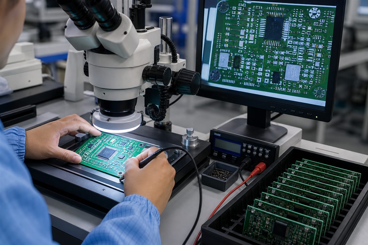
For assembled boards, add AOI, X-ray for hidden joints when needed, in-circuit testing, functional testing, programming verification, cleaning checks, and traceability. The right test plan depends on product risk, production volume, component package type, and field reliability requirements.
Common Mistakes When Ordering a Custom PCB
The most expensive ordering mistakes are usually file mismatches, unclear specifications, missing assembly data, and design choices that exceed normal fabrication limits.
- Uploading old Gerber files after the schematic or BOM changed.
- Forgetting the board outline, drill file, or stackup note.
- Using a footprint that does not match the real component package.
- Leaving polarity, pin 1, or connector orientation unclear.
- Choosing a surface finish without considering fine-pitch assembly or shelf life.
- Ignoring copper weight, temperature rise, and trace width for power circuits.
- Requesting controlled impedance without a confirmed stackup.
- Assuming prototype acceptance automatically proves mass-production stability.
How to Choose a Custom PCB Manufacturer
Choose a custom PCB manufacturer by matching the supplier’s proven capability to your board structure, quality requirements, assembly needs, documentation process, and communication speed.
Ask for a capability sheet, DFM feedback process, available materials, surface finishes, test methods, tolerances, controlled-impedance support, assembly options, sample approval process, packaging method, and change-control procedure. For regulated, automotive, medical, aerospace, or safety-related products, verify the exact certifications and compliance requirements directly with the supplier before ordering.
A good supplier should be willing to question unclear drawings, risky spacing, incomplete files, and inconsistent BOM data. That engineering feedback is often more valuable than a fast quote alone.
Custom PCB Pre-Order Checklist
A short pre-order checklist can prevent most avoidable PCB fabrication and assembly delays.
- Confirm schematic, layout, BOM, and production files are from the same revision.
- Run DRC in the PCB design tool and review manufacturer DFM warnings.
- Check board outline, mounting holes, connector positions, and enclosure fit.
- Confirm layer stackup, material, copper weight, thickness, solder mask, and finish.
- Mark impedance, high-voltage clearance, heavy-current traces, and test points clearly.
- Verify polarity, pin 1 marks, component rotations, and assembly drawings.
- Define inspection, electrical test, functional test, packaging, and labeling needs.
- Keep a controlled revision record for prototype, engineering validation, and mass production.
FAQ About Custom PCBs
Is a custom PCB the same as a prototype PCB?
No. A custom PCB describes a board designed for a specific product or circuit, while a prototype PCB describes an early build used for testing. A prototype can be custom, but the same custom design may later move into pilot production and mass production after validation.
Can I order a custom PCB without a schematic?
You can order bare boards if the Gerber or ODB++ files are complete, but the schematic is useful for engineering review and troubleshooting. For PCB assembly, the supplier also needs BOM and placement data. Without source design files, design changes and root-cause analysis become harder.
What is the difference between PCB fabrication and PCB assembly?
PCB fabrication makes the bare printed circuit board. PCB assembly, often called PCBA, mounts and solders components onto that bare board. If you need a working electronic module, you usually need both fabrication and assembly, plus testing or programming where required.
Which surface finish is best for a custom PCB?
There is no single best finish. HASL is common for many general boards, ENIG is often used for fine-pitch components and flat pads, OSP can suit cost-sensitive assembly, and other finishes may fit special needs. Choose based on component pitch, soldering process, storage time, reliability target, and budget.
How long does custom PCB manufacturing take?
Lead time depends on board complexity, material availability, quantity, factory loading, inspection needs, and shipping method. Simple prototype boards may be available quickly, while HDI, rigid-flex, special material, controlled-impedance, or high-reliability projects usually need more engineering and production time.
What causes most custom PCB delays?
Common causes include missing drill files, unclear board outlines, inconsistent revisions, unavailable components for PCBA, stackup questions, DFM violations, unconfirmed impedance requirements, and late design changes. Clean documentation and early supplier review reduce these delays.
Do I need IPC standards for every custom PCB?
Not every low-risk prototype needs formal IPC class documentation, but IPC references are useful for setting design, fabrication, assembly, and inspection expectations. For production or high-reliability projects, specify the required standards and acceptance class clearly in the procurement documents.
Can a custom PCB reduce product cost?
Yes, especially at volume. A custom PCB can remove extra wiring, adapters, connectors, and manual assembly steps. It may cost more during design and prototyping, but it can lower unit cost and improve repeatability once the product design is stable.
What should I send to a supplier for a PCBA quote?
Send fabrication files, BOM, pick-and-place data, assembly drawing, test requirements, quantity, target lead time, and any special component sourcing rules. Mark alternates and do-not-substitute parts clearly so the supplier does not make silent changes.
How do I know whether my custom PCB is manufacturable?
Run design-rule checks in your PCB software, compare the layout with the manufacturer’s capability sheet, and request a DFM review before production. Pay attention to spacing, hole sizes, annular rings, solder mask openings, copper balance, stackup, and assembly clearances.
Final Takeaway
A custom PCB is the product-specific hardware platform that turns a proven circuit into a manufacturable board. It gives engineers control over fit, routing, materials, testing, assembly, and repeatability, but it also requires clean production files and disciplined supplier communication.
If you’re sourcing reliable PCB/PCBA manufacturing, including OEM, ODM, prototyping, mass production, or custom engineering solutions, reach out to our engineering team for technical support and a quote at [email protected].



0 Comments