




If you are new to PCB layout, copper pour can look a little strange at first. You finish routing the traces, click a button in your PCB design software, and suddenly the empty areas of the board are filled with copper. It may feel like decoration, or simply a way to “use up” blank space.
In real PCB design, copper pour is much more than a visual fill. It can affect grounding, signal return paths, heat spreading, EMI behavior, current capacity, soldering, and even how easily the PCB can be manufactured.
A copper pour in PCB design is a filled copper area placed on a PCB layer and connected to a selected electrical net, most commonly ground. When used correctly, it can improve electrical and thermal performance. When used carelessly, it can create floating copper islands, poor return paths, unwanted coupling, or soldering problems.
This guide explains copper pour from a practical beginner’s point of view: what it is, why designers use it, the difference between solid and hatched copper, and the common mistakes worth avoiding before sending your board to fabrication.
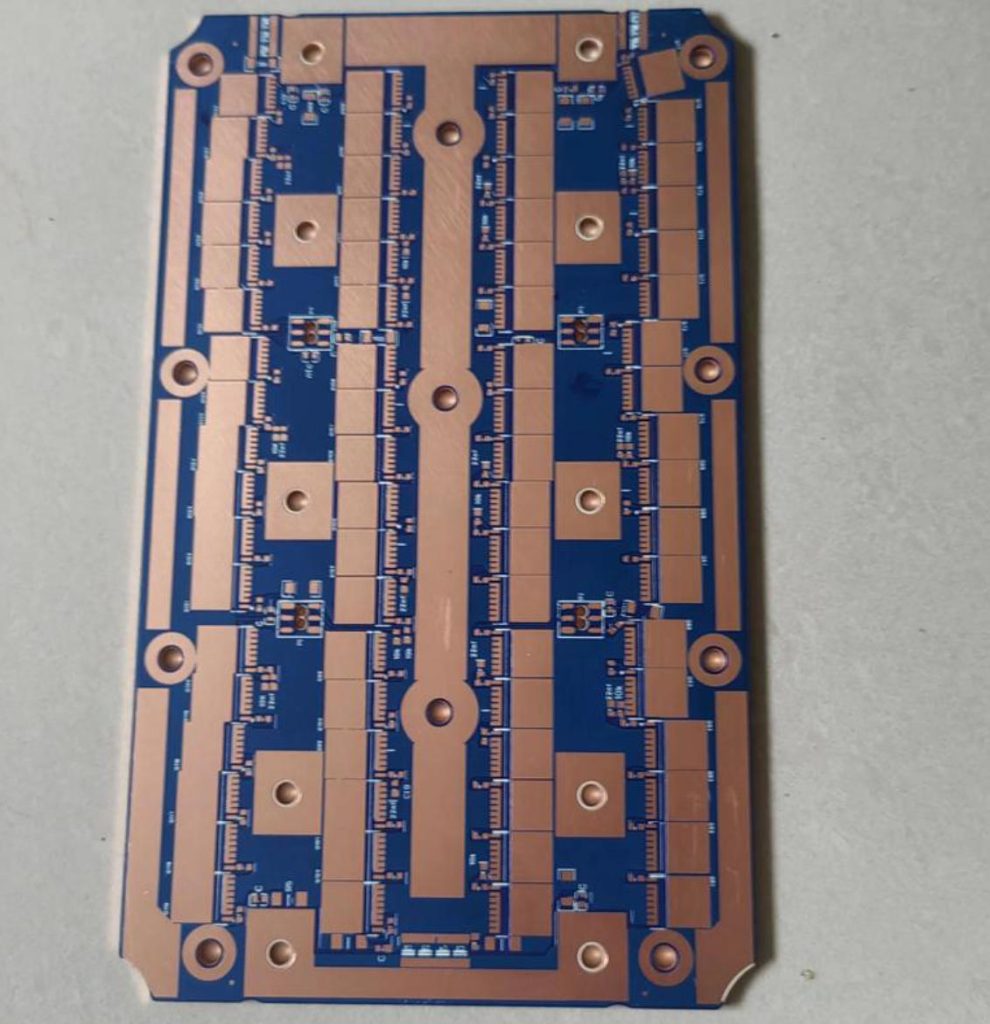
What Is Copper Pour in PCB Design?
Copper pour, also called copper fill, polygon pour, copper zone, or copper flood, is an area of copper added to a PCB layer. Instead of being a narrow trace, it is a larger copper region that fills available space while respecting clearance rules around other nets.
In most designs, copper pour is connected to ground. For example, after routing all the signal and power traces on a two-layer PCB, the designer may pour ground copper on the top layer, bottom layer, or both. The PCB software then fills the open areas with copper connected to the GND net, while keeping the required spacing from other traces, pads, vias, and components.
Copper pour can also be connected to other nets, such as:
- Power rails, such as 3.3V, 5V, or 12V
- High-current power paths
- Battery input nets
- Motor driver outputs
- Analog ground or power ground regions
- Thermal pads under power components
The key point is that copper pour should belong to a defined net. It should not just be random copper floating on the board. Floating copper may look harmless, but in some designs it can pick up noise, couple signals, or behave unpredictably.
Why Is Copper Pour Used in PCB Layout?
Copper pour is used for several reasons. Sometimes it is added for electrical performance. Sometimes it helps with heat. Sometimes it improves copper balance during manufacturing. In many real designs, it does several of these things at the same time.
Let’s look at the most common reasons designers use copper pour.
Copper Pour Can Improve the Signal Return Path
Every signal current needs a return path. Beginners often focus only on the visible signal trace, but the return current is just as important. In many PCB layouts, especially digital circuits, the return current flows through the nearest reference conductor, usually ground.
A well-connected ground pour can provide a shorter, lower-impedance return path. This helps reduce loop area, which can lower noise and unwanted radiation. On a simple two-layer PCB, using ground pour on both layers and connecting them with stitching vias is often better than leaving large empty areas with no useful copper.
However, copper pour is not magic. It only helps if it is continuous and properly connected. A ground pour that is chopped into thin, broken pieces may not provide a good return path at all. In some cases, it can make the return current take a longer route around slots, gaps, or isolated areas.
For high-speed signals, a clean and continuous reference plane is usually more important than simply filling every empty space with copper. If a fast signal crosses a split or void in the reference copper, the return path is interrupted, and that can increase EMI and signal integrity problems.
2. Copper Pour Helps Create a Lower-Impedance Ground
Ground is the most common net used for copper pour. A larger ground area usually has lower resistance and lower inductance than a thin ground trace. This is useful in many circuits, from simple microcontroller boards to power electronics and mixed-signal designs.
On a two-layer PCB, designers often pour ground on both the top and bottom layers. Then they add ground stitching vias to connect the two copper areas together. This creates a stronger ground network and gives return current more paths to flow.
For beginner designs, one common mistake is to split ground too aggressively. Some designers separate analog ground, digital ground, and power ground without fully understanding where the current will return. In many cases, a solid, well-planned ground system is safer than several poorly connected ground islands.
Ground partitioning can be useful, but it should be based on current flow, noise sources, and component placement—not just because a schematic has different ground names.
Copper Pour Can Help Spread Heat
Copper conducts heat much better than PCB laminate. That is why copper pour is often used around components that generate heat, such as voltage regulators, MOSFETs, motor drivers, LED drivers, power diodes, and charging ICs.
A larger copper area connected to a thermal pad or power pad can help spread heat across the board. If thermal vias are added, heat can move to other copper layers or to the opposite side of the PCB. This is a common technique for compact boards where there is no space for a large heatsink.
That said, copper pour does not automatically solve every thermal problem. The real cooling result depends on copper area, copper thickness, board thickness, via design, airflow, component package, and how much heat the device produces.
There is also a soldering trade-off. If a small pad is directly connected to a large copper pour without thermal relief, the copper can pull heat away during soldering. This may make the joint harder to solder, especially in hand soldering or selective soldering. For many through-hole pads and small SMD pads, thermal relief spokes are used to make soldering more reliable.
Copper Pour Can Reduce EMI When It Is Properly Grounded
A grounded copper pour can help reduce electric field coupling and provide some shielding. This is one reason ground copper is often placed around sensitive analog circuits, crystal oscillators, RF sections, and noisy switching power supplies.
But shielding only works when the copper is connected well to ground. A long, narrow, poorly connected piece of copper may not behave like a shield. It may behave more like an unintended antenna. This is especially important near high-frequency circuits or fast switching nodes.
If copper pour is used for EMI control, pay attention to via stitching. Ground vias placed around board edges, connectors, sensitive traces, or noisy areas can help tie copper areas together and reduce high-frequency impedance.
In switching power supplies, be careful when pouring copper near the switch node. The switch node is noisy and changes voltage quickly. Making that copper area too large can increase noise coupling. In many layouts, the switch-node copper should be kept compact, while ground copper is used carefully around it.
Copper Pour Can Carry More Current Than a Narrow Trace
For power nets, copper pour is often used instead of a thin trace. A wide copper region has lower resistance and can carry more current with less voltage drop and less heating.
This is common in:
- Battery-powered devices
- Motor control boards
- LED lighting boards
- Power supply PCBs
- High-current connectors
- Charging and protection circuits
Still, a copper pour should be designed with a clear current path. A large copper shape with a narrow neck can become a bottleneck. The current may still be forced through a small section, creating heat and voltage drop.
When using copper pour for current carrying, check the narrowest points, via count, copper thickness, connector pad design, and heat rise. Do not judge the current capacity only by the largest visible copper area.
Copper Pour Helps Balance Copper Distribution for Manufacturing
Copper distribution matters during PCB manufacturing. If one area of the board has a lot of copper and another area has very little, the board may be more difficult to etch evenly. Uneven copper can also contribute to warpage, especially on thin boards, large panels, or boards with heavy copper.
Copper pour can help make copper distribution more balanced across the PCB. This can improve manufacturing stability and reduce the chance of some process-related issues.
This does not mean every empty space must be filled without thinking. It means copper should be used in a controlled way, with proper spacing, clear net assignment, and good connection strategy.
Solid Copper Pour vs Hatched Copper Pour
When adding copper pour, PCB software may offer different fill styles. The two most common are solid copper pour and hatched copper pour.
Solid Copper Pour
Solid copper pour fills the selected area with continuous copper. It is the most common choice for modern PCB designs.
Solid pour is usually preferred when the goal is:
- Lower ground impedance
- Better return current path
- Higher current carrying capability
- Better heat spreading
- More effective shielding
- Cleaner manufacturing output
For most beginner PCB designs, solid ground pour is the better default choice, as long as it does not create soldering or layout problems.
Hatched Copper Pour
Hatched copper pour uses a grid or mesh pattern instead of a fully solid copper area. It was more common in older PCB processes or in special cases where designers wanted less copper coverage.
Hatched pour may be used when:
- Flexibility is needed on a flexible PCB
- Reduced copper density is desired
- Mechanical stress needs to be lowered
- A specific manufacturing or design requirement calls for it
For normal rigid PCBs, hatched copper is usually not the first choice for ground performance. The mesh pattern has higher impedance than solid copper and is less effective for high-frequency return paths and shielding.
| Type | Best Used For | Main Advantages | Possible Drawbacks |
|---|---|---|---|
| Solid Copper Pour | Ground, power, heat spreading, shielding | Low impedance, good thermal performance, better current capacity | Can make soldering harder if thermal relief is not used where needed |
| Hatched Copper Pour | Special cases, some flexible circuits, reduced copper density | Less copper coverage, more flexibility in some designs | Higher impedance, weaker shielding, less effective heat spreading |
Is Copper Pour the Same as a Ground Plane?
Copper pour and ground plane are related, but they are not always the same thing.
A ground plane usually means a large, continuous copper layer dedicated mainly to ground. In a four-layer PCB, for example, one internal layer may be used as a solid ground plane. This gives signals a stable reference and provides a low-impedance return path.
Copper pour is more general. It can be placed on outer layers or inner layers, and it can connect to ground, power, or another net. A copper pour connected to ground can act like part of a ground plane, but if it is broken into small pieces or poorly stitched, it will not perform like a true continuous plane.
For two-layer boards, ground copper pour is often used because there is no dedicated internal ground plane. For four-layer and higher-layer boards, a continuous internal ground plane usually gives better and more predictable performance.
Should Copper Pour Always Be Connected to Ground?
No. Copper pour does not always have to be connected to ground, but ground is the most common and often the safest choice.
A copper pour may be connected to a power rail when the purpose is to carry current or reduce voltage drop. It may also be connected to a thermal pad or a high-current output net. In power electronics, copper pour is often used for both ground and power paths.
What you generally want to avoid is unconnected copper. Floating copper islands can pick up noise and create unwanted capacitive coupling. Many PCB design tools have an option to remove isolated copper islands. For most beginner designs, enabling that option is a good idea.
If you decide to keep floating copper for a specific reason, make sure there is a real engineering purpose behind it.
What Are Thermal Reliefs and Why Do They Matter?
Thermal relief is a pad connection style where a pad connects to a copper pour through narrow copper spokes instead of being fully connected to the surrounding copper.
The purpose is simple: make soldering easier. If a pad is directly connected to a large copper area, the copper can absorb heat quickly. During soldering, the pad may not reach the right temperature as easily as nearby pads. This can lead to poor wetting, cold joints, or uneven soldering.
Thermal relief is commonly used for through-hole pads, connector pins, and some surface-mount pads connected to large pours.
Direct connection is still useful in some cases, especially for high-current pads or thermal pads under power components. The decision depends on whether electrical, thermal, or soldering performance is more important for that specific pad.
Common Copper Pour Mistakes Beginners Should Avoid
Copper pour is useful, but it can also create problems when added without checking the details. Here are some common mistakes seen in beginner PCB layouts.
1. Leaving Floating Copper Islands
Floating copper islands are copper areas that are not connected to any net. They may happen when the pour is cut off by traces, clearances, or board features. These islands can pick up noise or create unpredictable coupling.
In most cases, remove isolated copper islands or connect them properly to ground with vias.
2. Pouring Ground but Forgetting Stitching Vias
On a two-layer board, top and bottom ground pours should usually be connected with enough stitching vias. Without vias, the copper on each layer may not work together effectively.
Add ground vias near connectors, decoupling capacitors, signal layer changes, board edges, and noisy circuits. The exact spacing depends on the design, but the idea is to avoid long, poorly connected ground sections.
3. Creating Narrow Copper Necks
A pour may look large, but the actual current path may pass through a thin copper neck. This is a common issue around pads, slots, mounting holes, and dense routing areas.
Check the narrowest parts of power pours and ground connections. A bottleneck can heat up or create unwanted voltage drop.
4. Breaking the Return Path Under Fast Signals
If a signal trace runs over a gap in the reference copper, the return current must find another way around the gap. This increases loop area and can create EMI problems.
For fast digital signals, clocks, USB, RF traces, and other sensitive signals, keep the reference copper continuous under or near the trace whenever possible.
5. Pouring Copper Too Close to High-Voltage Nets
Copper pour must respect clearance and creepage requirements. This is especially important in high-voltage, AC input, power supply, and isolation designs.
Do not rely only on the default clearance setting. Make sure the clearance rules match the working voltage, safety requirement, pollution environment, and applicable design standard.
6. Connecting Every Pad Directly to Large Copper
Direct copper connection can be good for heat and current, but it may make soldering harder. If one pad of a small component connects to a large copper pour and the other pad does not, the two pads may heat unevenly during reflow.
This can sometimes contribute to tombstoning or poor solder joints on small passive components. Thermal relief and balanced pad design can help.
7. Assuming Copper Pour Fixes Poor Placement
Copper pour cannot rescue a bad layout. If decoupling capacitors are far from IC pins, high-current loops are large, or switching nodes are routed carelessly, adding copper at the end will not solve the main problem.
Good placement, short current loops, proper stackup, and clear routing still come first.
How Copper Pour Affects PCB Manufacturing
From a manufacturing point of view, copper pour is not just an electrical feature. It changes the copper distribution across the PCB, and that can affect etching, plating, solder mask, surface finish, warpage, and assembly behavior.
A well-designed copper pour can help create a more balanced copper layout. But very uneven copper distribution, large solid copper on one side, or heavy copper concentrated in one area may increase the risk of board bow and twist, especially on thin boards.
Copper pour can also influence solder mask openings and soldering. Large copper areas near fine-pitch pads need proper clearance and solder mask design. If the spacing is too tight, it may increase the risk of solder bridging or mask slivers.
Before fabrication, it is worth checking:
- Minimum copper clearance
- Minimum copper width and neck-down areas
- Isolated copper removal
- Thermal relief settings
- Clearance around mounting holes and board edges
- Copper balance between layers
- High-voltage creepage and clearance
- Whether copper pour creates acid traps or difficult etching features
If the PCB has heavy copper, high current, controlled impedance, high voltage, RF layout, or strict reliability requirements, it is better to review the copper pour strategy before production rather than after a board issue appears.
Practical Tips for Using Copper Pour
For beginners, the best copper pour strategy is usually simple and controlled. Do not add copper randomly just because the board looks empty. Use copper to support the electrical and thermal needs of the design.
- Use ground pour as the default choice for unused areas in many low- and medium-speed designs.
- Connect ground pours on different layers with stitching vias.
- Remove isolated copper islands unless there is a clear reason to keep them.
- Keep return paths continuous under important signals.
- Use thermal relief where solderability matters.
- Use direct connections where current or heat transfer is more important.
- Check narrow necks in high-current pours.
- Keep noisy switching copper compact.
- Respect clearance rules for high-voltage circuits.
- Review copper balance if the board is thin, large, or uses heavy copper.
After adding copper pour, always repour or refill the copper before generating Gerber files. Then inspect the final Gerbers, not only the PCB editor view. Many layout mistakes become easier to spot in the manufacturing files.
When Should You Avoid or Limit Copper Pour?
Copper pour is common, but more copper is not always better. There are times when copper should be limited or carefully shaped.
You may need to avoid or reduce copper pour:
- Near high-impedance analog nodes where leakage or coupling matters
- Around sensitive RF structures unless the layout is designed for it
- Near fast switching nodes that can capacitively couple noise
- Across isolation barriers or high-voltage gaps
- Where copper would create long floating sections
- Where soldering becomes difficult due to excessive heat sinking
- Where it disrupts controlled impedance routing
Copper pour should support the design goal. If it does not help the return path, heat flow, shielding, current capacity, or manufacturing balance, it may not need to be there.
FAQ: Copper Pour in PCB Design
What does copper pour mean in PCB design?
Copper pour means filling an area of a PCB layer with copper and connecting it to a selected net, such as ground or power. It is used to improve grounding, return paths, heat spreading, EMI behavior, current capacity, or copper balance.
Is copper pour necessary for every PCB?
Not always. Many PCBs benefit from copper pour, especially ground pour, but it should be added for a clear reason. Very simple boards may work without it, while high-speed, high-current, or thermally demanding boards often need careful copper planning.
Should copper pour be connected to ground?
Ground is the most common choice because it can improve return paths and reduce ground impedance. However, copper pour can also be connected to power or high-current nets when needed.
What is the difference between copper pour and ground plane?
A ground plane is usually a large, continuous copper area dedicated to ground, often on an internal layer. Copper pour is a broader term and can be used on any layer for ground, power, or other nets. A ground copper pour can act like part of a ground plane if it is continuous and well connected.
Is solid copper pour better than hatched copper pour?
For most rigid PCB designs, solid copper pour is better for grounding, current carrying, heat spreading, and shielding. Hatched copper is more suitable for special cases, such as some flexible PCB designs or specific copper density requirements.
Can copper pour cause problems?
Yes. Poorly designed copper pour can create floating islands, broken return paths, soldering difficulties, unwanted coupling, EMI issues, or high-current bottlenecks. Copper pour should always be checked as part of the final layout review.
What are stitching vias?
Stitching vias are vias used to connect copper pours on different layers, usually ground pours. They help reduce impedance and make the ground network more continuous.
What are thermal reliefs in copper pour?
Thermal reliefs are narrow copper connections between a pad and a copper pour. They reduce heat loss during soldering, making the pad easier to solder while still keeping it electrically connected.
Final Thoughts
Copper pour is one of those PCB layout features that looks simple but has a lot behind it. Used well, it can improve grounding, return current flow, thermal performance, EMI control, current capacity, and manufacturability. Used poorly, it can add problems that are hard to see until the board is built and tested.
For beginners, the best approach is not to pour copper everywhere blindly. Start with a clear purpose. Use ground pour where it supports return paths. Add stitching vias where layers need to work together. Use thermal relief where soldering matters. Remove isolated islands. Check high-current necks and high-voltage clearances before sending the design to fabrication.
A clean copper pour strategy makes a PCB more reliable, easier to manufacture, and easier to debug. It is a small layout detail that often has a big effect on the final board.



0 Comments