




To make a custom PCB, finish the circuit design, export clean Gerber and drill files, confirm the board specifications, run a manufacturability review, and then compare the quote assumptions before approving production. The board manufacturer cannot judge price, lead time, or risk correctly from a screenshot or schematic alone; the quote needs fabrication files and clear engineering requirements.
This guide is written for buyers, hardware engineers, and product teams who already know the circuit goal and now need to turn it into a buildable PCB order.
What does making a custom PCB actually involve?
Making a custom PCB means converting a product-specific circuit layout into manufacturing data that a PCB factory can fabricate, inspect, and, if needed, assemble.
The practical workflow is simple, but each step affects cost and production risk: design the schematic, lay out the board, export manufacturing files, choose board specs, check DFM issues, request a quote, review the quote details, and approve production. The common mistake is treating a custom PCB as only a design task. In manufacturing, it is also a file-control, tolerance, material, and communication task.
Which design files do you need before a manufacturer can quote?
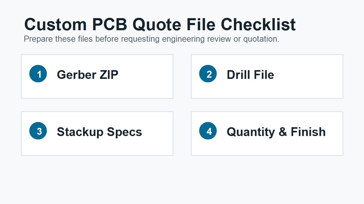
A manufacturer normally needs Gerber files, drill files, and clear board specifications before it can quote a custom PCB accurately.
| File or information | Why it matters | Buyer check |
|---|---|---|
| Gerber ZIP | Defines copper, solder mask, silkscreen, paste, and board outline layers. | Confirm every layer is exported and named clearly. |
| Drill file | Defines plated and non-plated holes. | Check drill units and whether slots are included. |
| Stackup notes | Controls layer count, dielectric thickness, impedance, and copper structure. | Use a factory-confirmed stackup for controlled impedance boards. |
| Board specs | Controls material, thickness, copper weight, surface finish, solder mask, and tolerance. | Do not leave critical specs as defaults. |
| Quantity and delivery target | Affects panelization, lead time, and unit cost. | Ask whether prototype and production quotes use the same assumptions. |
If you are not sure whether your export package is complete, review the basics of Gerber files for PCB manufacturing before requesting a quote.
What board specifications should be confirmed before fabrication?
The most important custom PCB specifications are layer count, material, board thickness, copper weight, surface finish, solder mask color, minimum trace and space, minimum hole size, impedance requirements, and final quantity.
Engineering teams should pay close attention to specs that are not easy to change later. Board thickness affects enclosure fit and connector alignment. Copper weight affects current capacity and etching difficulty. Surface finish affects assembly, storage life, and contact reliability. If the PCB will be assembled, confirm paste layer quality and component-side requirements early instead of after the fabrication quote is approved.
How do DFM checks reduce custom PCB production risk?
A DFM check catches manufacturing problems before the board moves into production, when correction is cheaper and faster.
Typical DFM issues include missing outline data, unclear slots, annular ring risk, copper-to-edge clearance, solder mask slivers, mismatched drill files, unsupported trace width, and spacing below the factory process limit. For custom boards, DFM is especially important because the design may not follow a standard product template. A short DFM check before PCB manufacturing can prevent avoidable remake cost and schedule delay.
What design checks should be finished before sending files?
Before sending custom PCB files for quote, finish the design checks that affect manufacturability, assembly, and first prototype risk.
This does not mean the factory replaces the design engineer. It means the file package should be mature enough for a manufacturer to review production risk instead of guessing the design intent. Use this pre-quote checklist before sending the Gerber ZIP.
| Check before RFQ | What to confirm | Why it protects the order |
|---|---|---|
| Schematic review | Power pins, reset pins, connectors, protection parts, and test points are not missing. | Prevents a buildable board with an electrical design mistake. |
| Footprint review | Pad size, pin 1, exposed pad, connector direction, and mechanical outline match the datasheet. | Reduces wrong-footprint and reversed-connector failures. |
| DRC pass | Trace width, spacing, drill size, copper-to-edge clearance, solder mask, and unrouted nets are checked. | Stops avoidable fabrication holds before the supplier quote. |
| Gerber viewer check | Board outline, copper layers, solder mask, silkscreen, drill files, and file origin are visually confirmed. | Catches outdated or incomplete manufacturing data. |
| Stackup and impedance | Layer count, material, copper weight, dielectric thickness, and impedance assumptions are ready for factory review. | Prevents quoting against a stackup the factory cannot build consistently. |
How should you compare custom PCB quotes?
Compare custom PCB quotes by checking whether each supplier quoted the same files, quantity, material, copper weight, surface finish, testing scope, and delivery condition.
A lower number is not always the lower-risk choice. One quote may exclude electrical testing, special material, impedance control, panelization, tooling, or assembly preparation. Another may include engineering review but use a longer lead time. When comparing PCB cost factors, ask what changed if a price is much lower than the others.
- Confirm whether the quote is for bare PCB fabrication only or includes assembly support.
- Check whether lead time starts after file approval, payment, material arrival, or engineering confirmation.
- Ask whether impedance, electrical testing, and special inspection are included.
- Confirm whether the same quote assumptions can support repeat production.
When should you add assembly, testing, or panelization?
Add assembly, testing, or panelization planning when the board will move beyond a bare PCB prototype into a working product build.
If components will be mounted, send the BOM and placement data together with the PCB files. This allows the supplier to check pad design, solder paste, component package fit, and assembly risk. For product builds, PCB assembly planning should not be delayed until after the bare PCB is fabricated, because assembly requirements can affect the PCB design itself.
For a first prototype, also plan the first-power check before production starts. The buyer or engineering team should inspect polarity, measure resistance between power and ground, use a current-limited bench supply, check voltage rails in sequence, and test one functional block at a time. These steps do not replace factory inspection, but they help avoid damaging components when the first assembled custom PCB is powered.
What common mistakes delay custom PCB production?
Most custom PCB delays come from file, footprint, and requirement mismatches rather than from the board shape itself.
- Using an outdated Gerber ZIP after the layout was revised.
- Forgetting the NC drill file or exporting drills in the wrong unit.
- Leaving the board outline unclear or duplicated across layers.
- Using a connector footprint with the correct pitch but wrong orientation.
- Omitting polarity marks for diodes, LEDs, electrolytic capacitors, or connectors.
- Choosing trace width, spacing, or via sizes below the intended factory capability.
- Sending assembly data without a BOM, CPL, or clear no-substitution rules.
- Missing test points for power rails, programming, reset, and critical signals.
What should you send PCBTRY for a file review?
For a useful custom PCB review, send the Gerber ZIP, drill files, board specifications, target quantity, delivery target, and any notes about impedance, material, assembly, testing, or enclosure constraints.
If you want PCBTRY to review a custom PCB before production, email the files and requirements to [email protected]. Include the Gerber ZIP, drill files, layer count, board thickness, copper weight, surface finish, quantity, delivery target, and any assembly notes. The team can check manufacturability, quote assumptions, and production risk before you approve the order.
FAQ
Can I make a custom PCB from only a schematic?
No. A schematic explains the circuit, but the factory normally needs PCB layout manufacturing files such as Gerber and drill files to fabricate the board.
Do I need a BOM for a bare custom PCB?
No, not for bare board fabrication. A BOM is required when the order includes component sourcing, SMT assembly, through-hole assembly, or turnkey PCBA service.
What is the safest way to start a custom PCB order?
Start with a small prototype quantity, confirm DFM comments, verify fit and function, and then move to production using the corrected files and stable specifications.
What is the difference between a custom PCB and a prototype PCB?
A custom PCB describes a board designed for a specific product or function. A prototype PCB is usually the first small batch used to verify that custom design before repeat production.
Which files should I check before asking for a custom PCB quote?
Check the Gerber ZIP, NC drill file, board outline, layer count, material, thickness, copper weight, surface finish, quantity, and any impedance or assembly notes.
Do I need a DFM review for a simple two-layer custom PCB?
Yes, a basic DFM review is still useful. Even simple boards can have unclear outlines, drill issues, copper-to-edge risk, solder mask slivers, or missing production notes.
When should I involve the PCB manufacturer?
Involve the manufacturer before the quote if the board has controlled impedance, special materials, heavy copper, tight spacing, assembly constraints, unusual thickness, or a schedule-sensitive prototype.
Can the manufacturer fix my Gerber files?
A manufacturer can sometimes suggest production edits, but the safest practice is to correct the source PCB layout and re-export the files so the design database stays consistent.
What causes custom PCB quote differences between suppliers?
Differences often come from material assumptions, copper weight, surface finish, testing scope, impedance control, panelization, lead time, and whether engineering review is included.
Should I order bare PCBs first or include assembly?
If the design is new and component risk is low, a bare PCB prototype can verify fit and fabrication first. If pad design, sourcing, or functional testing matters, include assembly review early.
What should I save for the next custom PCB revision?
Save the released Gerber ZIP, source CAD files, BOM, DFM comments, quote assumptions, test notes, rework records, and the final approved revision number.
What should I send PCBTRY to get useful feedback?
Send the Gerber ZIP, drill files, board specifications, quantity, delivery target, assembly notes, and any known design risks to [email protected].
Related PCB Guides
If you are using this guide to prepare a PCB project, these related PCBTRY guides can help you connect the next step instead of reading each topic in isolation.



1 Comment
When to Use an Evaluation Board vs Custom PCB Design: A Stage-Gate Guide - thindry pcb manufacturer · 08/23/2026 at 13:29
[…] expectations and test requirements. For related next steps, review PCBtry’s guides to custom PCB files and quote checks, moving a prototype into PCB design, and circuit-card assembly test […]