Blog
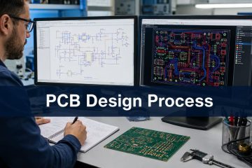
PCB Design Process: Requirements, Layout and Release Checks
Follow a practical PCB design process from requirements and schematic capture through stackup, placement, routing, verification, Gerber review and production release.



Follow a practical PCB design process from requirements and schematic capture through stackup, placement, routing, verification, Gerber review and production release.
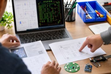
Learn PCB design through three beginner projects, from schematic and footprints to layout, ERC/DRC, manufacturing files, DFM and first-board checks.
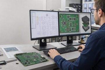
Learn how to create a PCB in Fusion 360 from schematic and board outline through layout, DRC, Gerber export and fabrication file checks.
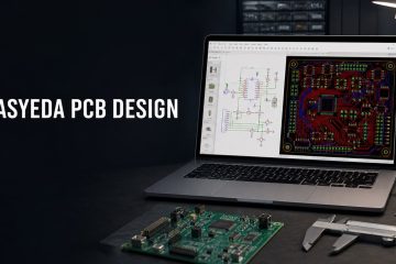
Learn how to use EasyEDA for PCB design from schematic and footprint checks through layout, DRC, Gerber export and manufacturing review.
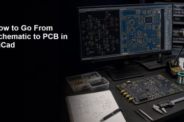
Learn how to go from schematic to PCB in KiCad with footprint checks, board outline setup, routing, DRC, Gerber export and DFM review.
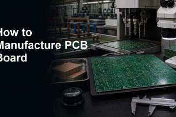
Learn how to manufacture PCB board from Gerber files through imaging, drilling, plating, solder mask, silkscreen, surface finish, inspection, and DFM checks.
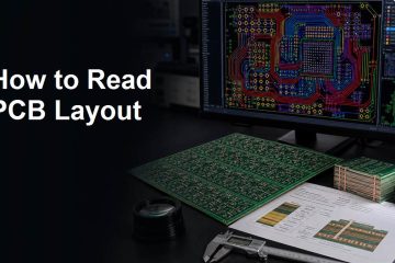
Learn how to read PCB layout files by checking board outline, layers, components, traces, vias, drill files, silkscreen, and DFM issues before fabrication.
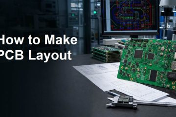
Learn how to make PCB layout from schematic and footprints to placement, routing, DFM checks, Gerber files and manufacturing review.
Learn how to design a PCB board for a circuit, from schematic and footprints to layout, DFM checks, manufacturing files and quote-ready review.
Learn how PCBs are made in a factory, from Gerber review and layer imaging to etching, drilling, plating, solder mask, surface finish and electrical testing.
If you have any enquiry about quotation or cooperation, please feel free to email us at [email protected] or use the following enquiry form. Oursales representative will contact you within 24 hours. Thank you for your interest in our products.