




HDI PCB China: Microvias, Stackup and DFM Quote Checks

An HDI PCB China project should not be quoted only by board size and layer count. Buyers need to confirm microvia structure, lamination cycle, impedance needs, via-in-pad rules, copper balance, copper thickness and balance, material selection, inspection scope and the files required for an accurate DFM review.
This guide is written for engineers and buyers preparing HDI PCB prototypes or low-volume production in China. It focuses on the practical decisions that affect yield, quotation accuracy, delivery risk and supplier comparison.
What Should Buyers Check First for an HDI PCB China Project?
Start by checking whether the design truly needs HDI construction. HDI is useful when the board has fine-pitch BGAs, high routing density, controlled impedance, small board size or many high-speed connections, but it adds process control requirements that a simple multilayer PCB may not need.
- Fine-pitch BGA breakout and via pitch.
- Layer count, signal density and power-plane needs.
- Microvia depth and whether stacked vias are required.
- Impedance-controlled nets and reference-plane continuity.
- Prototype quantity, test requirements and production target.
When Does a PCB Design Need HDI Instead of Standard Multilayer PCB?
A PCB design normally moves toward HDI PCB design when standard through-hole vias consume too much routing space or make BGA escape routing unstable. If the same circuit can be routed with conventional vias, wider design rules and fewer lamination steps, standard multilayer PCB may be safer and lower cost.
| Design signal | HDI relevance | Buyer action |
| 0.4 mm or fine-pitch BGA | Often needs microvia breakout | Send BGA package and fanout rules |
| High routing density | HDI can reduce via congestion | Review layer count and via structure |
| High-speed interfaces | May need impedance and return-path control | Provide impedance target and stackup request |
| Very small product enclosure | HDI can reduce board area | Confirm mechanical constraints early |
HDI PCB Stackup Decisions Before Quoting
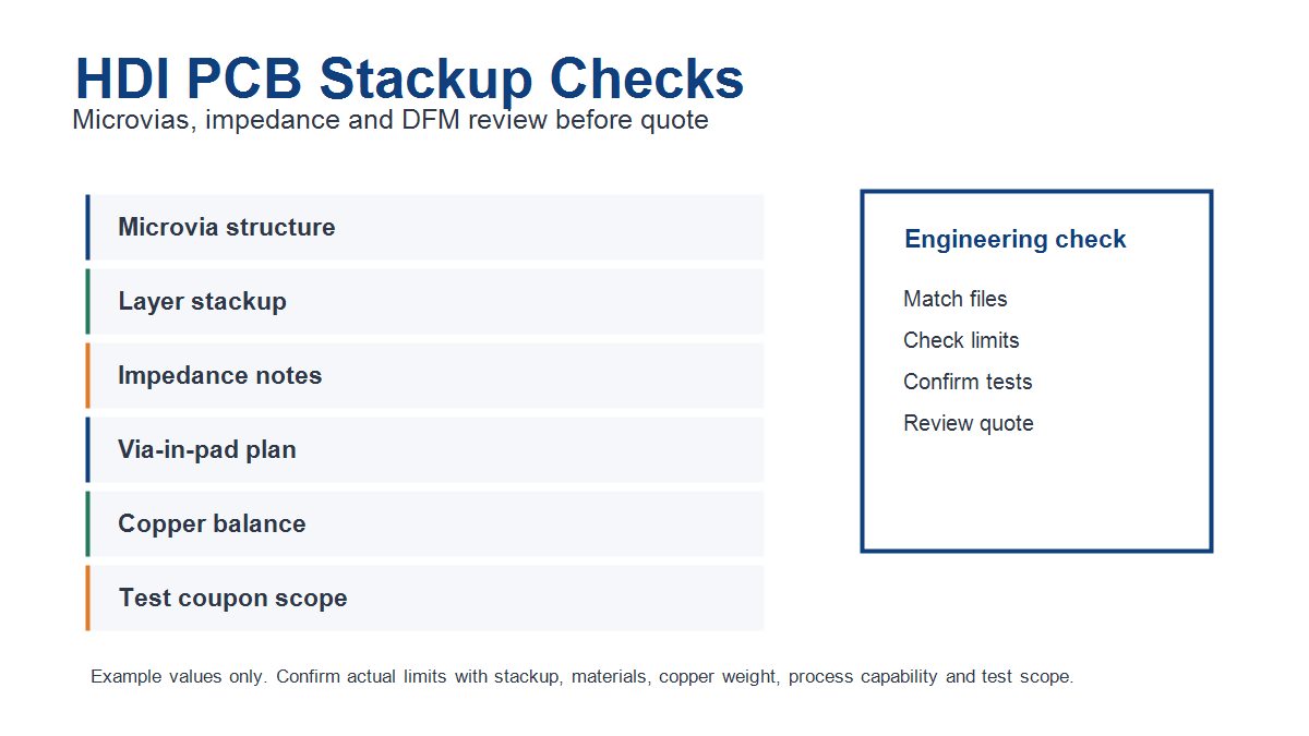
The stackup is one of the first items a China HDI PCB manufacturer should review. It affects lamination sequence, dielectric thickness, laser drilling depth, impedance, copper distribution and test coupon planning.
Microvia Structure: Blind, Buried, Stacked or Staggered?
Microvia structure changes both manufacturability and price. Staggered microvias are often easier to manufacture than stacked microvias, while stacked microvias may be needed when space is extremely limited. The quote request should state whether blind vias, buried vias, via-in-pad or stacked microvias are expected.
Why Lamination Cycle Matters in HDI PCB Manufacturing
HDI boards may need sequential lamination. More lamination cycles usually mean higher cost, longer lead time and tighter process control. Buyers should ask the supplier to confirm whether the proposed stackup uses one buildup, two buildups or a more complex sequence.
HDI PCB Material Choices for Signal and Reliability
Material choice should follow signal speed, loss requirements, Tg, CTI, thermal stress and assembly temperature. Do not choose a laminate only because it appears in another design. If controlled impedance or high-speed PCB design loss matters, send the stackup target and ask the supplier to confirm available material alternatives before release.
Impedance Control and Test Coupon Requirements
If an HDI board has impedance-controlled traces, the RFQ should include target impedance, tolerance, layer, trace geometry and reference plane. Ask whether impedance coupons will be built on the panel and whether the report will be included after production.
Via-in-Pad, Filling and Plating Checks
Via-in-pad can save space under fine-pitch components, but it needs clear filling, capping and plating instructions. Missing via-in-pad notes can cause solder voiding, uneven pads or quotation changes after DFM review.
Design Rules a China HDI PCB Manufacturer Should Confirm
Before production, confirm the minimum trace and space, laser via size, capture pad size, annular ring, solder mask bridge, copper-to-edge distance, aspect ratio and controlled-depth features. These limits should come from the actual supplier capability, not from a generic online design rule.
Common HDI PCB DFM Risks Buyers Should Avoid
Common risks include unsupported stacked microvias, unbalanced copper, overly tight solder mask dams, missing impedance notes, unclear buried-via layers, insufficient BGA escape space and incomplete drill files. DFM feedback should be reviewed before approving the order.
| Risk | Why it matters | What to send |
| Unclear microvia layers | Can change lamination sequence | Stackup and drill chart |
| Missing impedance target | Supplier cannot verify trace geometry | Impedance table and net list |
| Via-in-pad not specified | Can cause solder and filling issues | Via filling/capping notes |
| No test coupon request | Harder to verify impedance/process | Test report requirements |
HDI PCB Prototype vs Volume Production Checks
Prototype HDI boards should prove the stackup, microvia reliability, BGA assembly readiness and test method before volume release. A prototype that is rushed without DFM feedback may pass one build but create problems when quantity increases.
What Files Are Needed for an HDI PCB Quote?
A complete HDI RFQ should include Gerber or ODB++ files, NC drill files, stackup request, impedance table, fabrication drawing, via-in-pad notes, material requirements, surface finish, quantity, lead-time target and inspection requirements.
How to Compare HDI PCB China Quotes
Compare quotes by confirmed stackup, via structure, material availability, impedance support, testing scope, DFM comments, lead time and engineering communication. A lower price is not useful if it omits via filling, impedance coupon testing or the actual lamination sequence.
When Should You Ask PCBTRY for HDI PCB Engineering Review?
Ask for engineering review before ordering when the design uses fine-pitch BGAs, microvias, via-in-pad, controlled impedance, tight spacing or a compact enclosure. For bend or space-constrained boards, compare the requirement with rigid-flex PCB manufacturing before locking the stackup. Early review helps identify whether the board can be simplified, whether the stackup is realistic and what quote notes should be added.
FAQs About HDI PCB China
What is an HDI PCB? An HDI PCB is a high-density interconnect board that uses finer traces, smaller vias and often microvias to route dense components or compact electronics.
Is HDI always better than a standard PCB? No. HDI is useful for dense or high-speed designs, but standard multilayer PCB can be lower risk and lower cost when routing space is enough.
What is a microvia? A microvia is a small laser-drilled via, often used to connect adjacent layers or support fine-pitch BGA breakout.
Do HDI PCBs need special materials? Some do, especially high-speed or high-reliability designs. Material choice depends on signal loss, thermal stress, stackup and assembly conditions.
Why does via-in-pad increase cost? Via-in-pad often needs filling, capping and plating control, which adds process steps and inspection requirements.
What files help quote an HDI PCB accurately? Gerbers, drill files, stackup, impedance table, fabrication drawing and via instructions are the most important files.
Can a China HDI PCB supplier change my stackup? The supplier may suggest manufacturable alternatives, but engineering approval should happen before production data is released.
Should I order HDI prototypes before volume production? Yes, for most dense boards. Prototype builds help validate stackup, microvias, impedance and assembly risk.
How do I reduce HDI PCB cost? Avoid unnecessary stacked microvias, reduce lamination complexity, keep design rules realistic and provide complete files for DFM review.
When should I contact PCBTRY? Contact PCBTRY when your HDI design needs stackup review, microvia feasibility checks, impedance notes or a comparison quote before production.
Final RFQ Step
If you are sourcing HDI PCB manufacturing in China, send Gerber or ODB++ files, drill data, stackup notes, impedance requirements, via-in-pad instructions, quantity and lead-time target to [email protected]. PCBTRY can review manufacturability, quote risks and production requirements before you release the order.



0 Comments