




How Do You Mount a PCB in an Enclosure Safely?
To mount a PCB in an enclosure safely, first define the board position and external interfaces, then choose a mounting method, provide clearance above and below the board, decide whether any mounting point is electrically connected to the enclosure, and trial-fit the complete assembly before production. The PCB should be supported without bending, touching the enclosure floor, blocking airflow or forcing connectors into their panel openings.
In simple terms, the enclosure and PCB must be designed as one mechanical system. A board can pass electrical testing and still fail in the product because a screw head touches copper, a capacitor hits the lid, a USB connector misses its cutout, or a metal standoff creates an unintended ground connection.
A reliable sequence is:
Step 1: Freeze the board outline, mounting points, connector locations and tallest components.
Step 2: Choose standoffs, molded bosses, card guides, edge clips or another retention method that fits the service and vibration needs.
Step 3: Check board-edge, underside, lid, tool and cable clearances in the 3D assembly.
Step 4: confirm grounding, heat flow and mechanical load paths instead of treating the screws as purely mechanical parts.
Step 5: build and measure a trial assembly before releasing PCB and enclosure tooling.
What Must Be Decided Before PCB Layout Is Finished?
The enclosure constraints should be decided before the final PCB layout because they control board shape, hole locations, connector positions and component height. Waiting until routing is complete often forces a layout change or a new board revision.
Start with a mechanical constraint package. It should show the enclosure’s internal length, width and height; the PCB coordinate origin; mounting-boss or rail locations; wall thickness; lid features; connector cutouts; button, LED and display locations; cable bend space; and the areas that must remain clear for assembly tools.
For example, imagine a USB connector that must pass through a front-panel opening. The PCB designer cannot place it approximately near the edge and hope the enclosure absorbs the error. The connector centerline, PCB edge and panel cutout must use a shared reference. Otherwise, tolerance from the board outline, connector placement, standoffs and enclosure machining can all add in the same direction.
- Fix the external interfaces first: connectors, switches, displays, antennas and indicators.
- Place mounting holes and mechanical keep-outs before dense routing.
- Record the tallest top-side and bottom-side components.
- Decide whether the PCB will be installed from above, slid into rails or attached to a removable panel.
- Leave room for screwdrivers, nut drivers, cable plugs and service removal.
This mechanical information belongs with the electrical design inputs, not in a late email after the Gerber files are finished.
Which PCB Mounting Method Fits the Enclosure?
The right mounting method depends on board size, enclosure material, assembly volume, service access, vibration and whether the PCB already has mounting holes. Threaded standoffs are flexible, molded bosses reduce separate hardware, and slide-in rails make removal easy, but each option creates different PCB constraints.
| Mounting method | Best fit | Main PCB requirement | Common risk |
| Threaded standoffs | Metal or plastic enclosures, prototypes and serviceable products | Mounting holes, copper keep-outs and tool access | Board bending, loose hardware or unintended chassis ground |
| Molded bosses | Injection-molded plastic enclosures and repeat production | Hole pattern matched to the molded enclosure | Boss cracking, stripped threads or expensive mold changes |
| Slide-in card guides | Extruded enclosures and modular industrial equipment | Controlled board thickness and component-free edge strips | Rattle, excessive insertion force or blocked connectors |
| Snap clips or edge retainers | Small boards and fast assembly without loose screws | Defined board-edge engagement and flex limit | Clip stress, difficult service or damage during removal |
| Adhesive mounts | Low-load prototypes where drilling is not possible | Clean bonding surface and safe thermal environment | Ageing, heat release and poor reworkability |
Do not choose only by hardware price. A cheap clip that makes the board difficult to remove or a rigid four-point mount that twists across a warped panel can cost more during assembly and field repair.
How Do Mounting Holes and Keep-Out Areas Prevent Damage?
A mounting hole needs more than a drill diameter. It also needs a mechanical keep-out that protects copper, traces, components and solder joints from the screw head, washer, standoff body and installation tool.
The hole diameter should be selected from the actual fastener and the expected positional tolerance, not from the screw name alone. The keep-out must account for the largest hardware diameter and the tool needed to tighten it. A nut driver can require much more room than the nut itself.
Check every mounting point in the PCB layout and the Gerber output:
- No signal trace, via or component body should enter the hardware sweep area unless the design intentionally allows it.
- The screw head and washer must not scrape solder mask or press against a small component.
- Internal copper planes must have the intended clearance around a non-plated hole.
- Board-edge and mounting-hole tolerances must still allow all fasteners to start without forcing the PCB sideways.
- Heavy connectors should not rely on nearby solder joints as their only mechanical support.
If the board drawing only shows four circles and no keep-out definition, the mounting design is incomplete.
How Should Standoff Height and Board Clearance Be Chosen?
Standoff height should be based on the tallest feature below the PCB, required electrical isolation, airflow and enclosure geometry. Lid clearance should be based on the tallest top-side part plus assembly and component-height tolerances.
A practical calculation begins with actual component data. Measure or obtain the maximum height of bottom-side solder joints, connector pins, test points and components. Add the planned air or insulation margin, then select a standoff that keeps every conductive feature away from the enclosure floor. Repeat the check above the PCB for capacitors, transformers, heatsinks and cable plugs.
As a simple example, suppose the tallest bottom-side feature is 2.0 mm and the project requires 1.5 mm of additional clearance. The design needs more than 3.5 mm from the PCB underside to the enclosure floor after tolerances are included. This is an example, not a universal rule; the real margin depends on voltage, environment, component movement, coating, insulation and manufacturing capability.
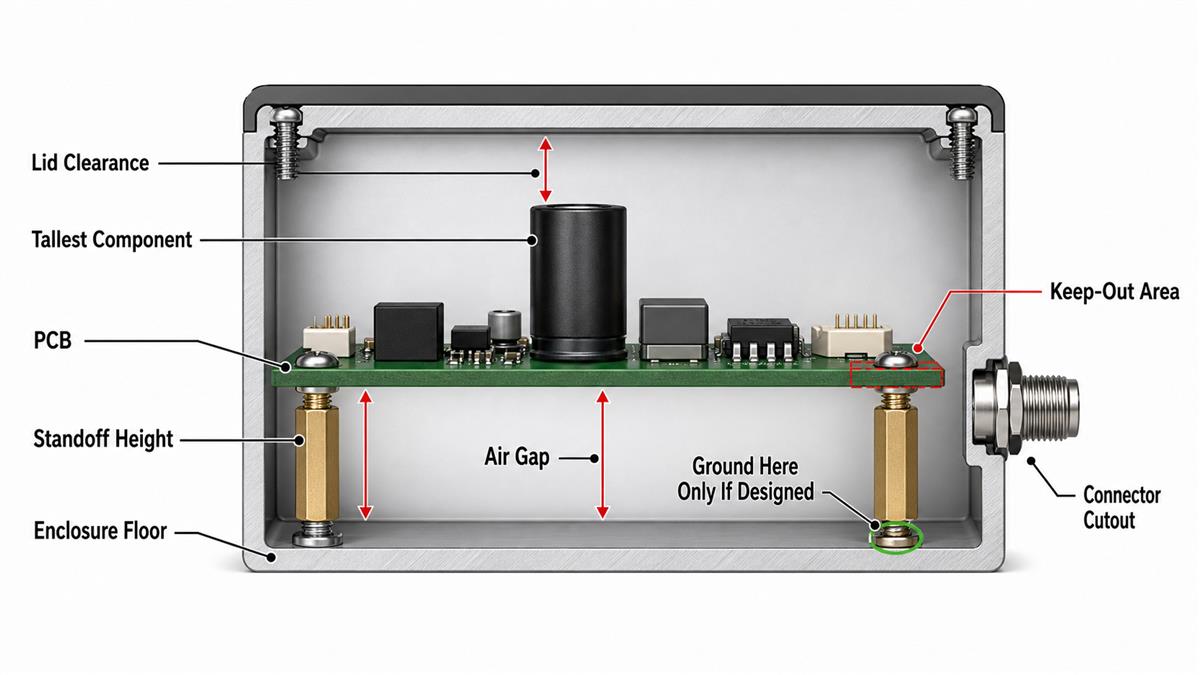
The drawing should state finished PCB thickness and the reference surface used for height calculations. Otherwise, one engineer may dimension from the board top while another dimensions from the enclosure floor.
How Do You Align Connectors, Switches and Display Cutouts?
External interfaces should be aligned from shared mechanical datums. That means the PCB holes, board edge and enclosure cutouts are measured from the same origin instead of being dimensioned through several unrelated features.
Place critical connectors first in the PCB mechanical model. Check the connector body, mating plug, cable bend radius, latch movement and the user’s insertion force. A connector can be centered in a cutout and still be unusable if the cable shell hits the wall or the latch cannot move.
Use this sequence:
Step 1: define the enclosure datum surfaces and the PCB origin.
Step 2: locate mounting points from those datums.
Step 3: locate connector centerlines and panel openings from the same datums.
Step 4: calculate worst-case position using PCB outline, hole, placement and enclosure tolerances.
Step 5: verify the fit with the real connector and mating cable, not only a simplified 3D block.
For frequent-mating connectors, consider a chassis support or bracket so insertion force is not carried only by solder joints.
When Should Mounting Holes Be Plated or Non-Plated?
Use a non-plated through hole when the mounting point is meant to be mechanically isolated from PCB copper. Use a plated mounting hole only when the electrical connection is intentional and the grounding strategy defines what that connection does.
| Hole choice | Typical purpose | What must be checked |
| NPTH with copper clearance | Pure mechanical attachment and electrical isolation | Internal plane clearance, hardware size, positional tolerance and washer area |
| Plated hole tied to chassis ground | Intentional low-impedance connection to a metal enclosure | Ground type, connection point, plating, hardware finish and contact reliability |
| Plated pad not connected to a net | Mechanical wear surface or optional connection | Whether fabrication and assembly documentation clearly describe the intent |
A common mistake is to connect every mounting hole to the circuit ground by habit. That can create multiple chassis connections, noise paths or confusion between signal ground, power return and protective earth. Another mistake is leaving a non-plated hole too close to an internal plane, where drilling tolerance could expose copper.
Show the decision in the schematic, PCB stackup and fabrication drawing so the manufacturer does not have to infer it.
How Should a Metal Enclosure Be Grounded?
A metal enclosure should be grounded according to the product’s power, safety and electromagnetic compatibility design, not simply because a metal screw touches a PCB pad. The correct connection may be protective earth, chassis ground, circuit ground through a controlled network, or no direct connection at a particular mounting point.
For a beginner, the important distinction is that “ground” is not always one identical node. Signal ground is the reference for circuit signals. Protective earth is a safety path. Chassis ground is the conductive enclosure. They may be connected, but the location and method matter.
Before approving plated mounting holes, ask:
- Which ground is this mounting point connected to?
- Is there one planned chassis bond or several parallel paths?
- Will paint, anodizing, washers or thread-locking material prevent metal contact?
- Can the connection remain reliable after vibration, corrosion and service?
- Does the product require a separate safety review or compliance test?
High-voltage or safety-critical equipment needs review by a qualified engineer against the applicable product requirements. A blog diagram cannot replace that project-specific analysis.
How Do You Control Heat Around an Enclosed PCB?
Thermal control starts by identifying where heat is generated and where it can leave the enclosure. Mounting height and board orientation affect airflow, while standoffs, metal walls and thermal interfaces can create or block heat paths.
Mark regulators, processors, power resistors, LEDs, transformers and other heat-producing parts in the mechanical model. Check whether the lid traps hot air above them, whether cables block vents, and whether a heatsink has room to receive airflow. If a component uses the enclosure as a heat spreader, define the pad, insulator, pressure and assembly method rather than relying on accidental contact.
A prototype should be tested in the closed enclosure at realistic load and ambient conditions. An open-board bench test can look healthy because room air reaches every component, while the same board overheats after the lid is installed.
Moisture protection can also change heat flow and serviceability. If the product uses coating, sealing or outdoor protection, review the related guidance on how to protect a PCB from moisture before finalizing vents and enclosure seals.
How Do You Design for Shock and Vibration?
Shock and vibration design prevents the PCB from moving, flexing or transferring repeated load into solder joints. Large boards, heavy components and cable-connected products usually need more support than a small, light board used on a desk.
Mounting points should restrain the board without creating a twist. Add support where the board spans a long distance or where a heavy transformer, heatsink or connector creates local load. Secure cables so they do not pull on headers. For slide-in rails, control side clearance and add an end stop or retainer so the board cannot rattle along the rail.
Potential failure signs include fretting marks around hardware, cracked solder joints near connectors, loose screws, worn card edges and intermittent operation when the product is moved. The appropriate vibration test depends on the product and its environment, so the acceptance profile must come from the project requirements rather than a generic blog value.
How Do You Prevent Board Flex and Fastener Damage?
Board flex is prevented by keeping support surfaces coplanar, tightening hardware evenly and avoiding excessive clamp force. A PCB should sit naturally on all supports before the screws are tightened.
| Failure | Likely cause | Production impact | Prevention check |
| PCB bows after tightening | Unequal boss height, warped panel or over-tightened screw | Cracked solder joints, stressed vias or intermittent faults | Check coplanarity and define an assembly torque/process |
| Solder mask scraped near hole | Wrong washer/head size or insufficient keep-out | Exposed copper and possible short to chassis | Model the complete hardware stack and tool envelope |
| Connector solder joints crack | Mating force transferred into PCB | Field failures and difficult intermittent faults | Add chassis support or strain relief where needed |
| Screw loosens in service | Vibration, unsuitable fastener or weak plastic thread | Rattle, loss of ground bond or short circuit | Choose a retention method compatible with service and material |
| Board cannot be installed | Hole pattern or cutout tolerance stack is too tight | Manual rework, forced assembly or scrap | Use shared datums and verify worst-case fit |
Do not publish a universal screw torque without the fastener, thread, washer, PCB material and enclosure details. The assembly drawing should instead identify the approved hardware and project-specific process.
How Can You Mount a PCB With No Mounting Holes?
A PCB with no mounting holes can be retained by card guides, edge clips, a surrounding cradle, a removable tray or a qualified adhesive mount. The chosen method must hold the board edges without pressing on components, traces or solder joints.
Rails work well when two opposite board edges are free of components and the board thickness matches the guide. A cradle can support several edges and include stops that prevent sliding. Snap clips can speed assembly, but they need controlled flex and a removal path. Adhesive mounts are better treated as an engineered material choice than as a default shortcut because heat, contamination, ageing and rework can weaken the bond.
Do not clamp directly onto ceramic components, soldered connectors or unsupported corners. If an existing module was not designed for enclosure mounting, make a physical sample and inspect where the retention force actually enters the board.
What Tolerances Must the PCB and Enclosure Share?
The PCB and enclosure must share tolerances for board outline, hole position, boss position, standoff height, connector placement, cutout location and component height. A nominal CAD fit is not enough because every manufactured feature varies.
Build a tolerance stack around each critical interface. For a panel connector, include the PCB outline tolerance, mounting-hole position, enclosure boss position, component placement tolerance, connector body tolerance and cutout machining or molding tolerance. Then check the worst practical combination, not only the average.
Use the same coordinate origin in the PCB mechanical drawing and enclosure drawing. Exchange a STEP model for visual interference review, but keep critical dimensions in controlled drawings because a 3D model alone may not communicate tolerance, plating, surface finish or revision.
If you need to inspect where mounting holes, edge cuts and components appear in the design, the guide on how to read a PCB layout explains the main physical layers and DFM checkpoints.
What Should Be Checked During a Trial Fit?
A trial fit should prove that the real PCB, real hardware, real enclosure and real cables can be assembled without force or interference. It should happen before committing to mass production or expensive enclosure tooling.
Step 1: place the PCB on the supports without screws. It should contact all intended supports without rocking.
Step 2: start every screw by hand. If holes only align after pushing the PCB sideways, the tolerance plan needs correction.
Step 3: tighten the approved hardware in the planned sequence while watching for board bow.
Step 4: install the lid and check top-side and bottom-side clearance with the complete component population.
Step 5: mate every connector, operate every switch, view every indicator and check cable bend space.
Step 6: power and thermally test the closed assembly under realistic load.
Step 7: inspect grounding continuity where a bond is required and isolation where it is not.
Step 8: remove and reinstall the PCB to confirm service access and that clips or threads are not damaged.
Photograph the approved assembly and record measured gaps, hardware and revision numbers. That evidence prevents a later supplier from reproducing only the nominal CAD arrangement.
What Files Should Be Sent for PCB and Enclosure Review?
A useful review package combines PCB manufacturing data with mechanical and assembly information. Gerber files alone show copper and mask, but they do not fully describe the enclosure interfaces or installation process.
- Gerber files, NC drill files and a clear board outline.
- PCB fabrication drawing with finished thickness, hole types, tolerances and mounting-hole notes.
- Stackup, copper weight, material and surface-finish requirements.
- STEP model of the PCB assembly with accurate component heights.
- Enclosure drawing or STEP model with bosses, rails, cutouts, vents and datum locations.
- BOM and assembly drawing when populated-board review is required.
- Connector datasheets and mating-part information.
- Grounding, thermal, vibration, coating and test requirements.
- Prototype quantity, production quantity and target revision.
Before sending the package, inspect the manufacturing outputs as a set. This factory-focused guide on how to manufacture a PCB board explains why drill, plating, solder mask, outline and electrical-test data must agree.
For boards supplied in arrays, also confirm that breakaway rails and tabs do not conflict with final enclosure edges; the PCB panelization guide covers those temporary production features.
FAQ About Mounting a PCB in an Enclosure
Should a PCB touch the bottom of a plastic enclosure?
No. Even in a plastic enclosure, standoffs or another support method should control the board position. Direct contact can press on solder joints, trap debris, block airflow and transfer enclosure flex into the PCB.
Are four mounting holes always enough?
Not always. Board size, thickness, heavy components, connector force and vibration determine support needs. A long board may need a center support, while a small light board may work with fewer points if the load path is controlled.
Can metal standoffs short a PCB?
Yes, if the standoff or screw touches exposed copper, an internal plane near the drill, a component lead or an unintended plated pad. Use defined keep-outs and decide whether the mounting point is isolated or grounded.
Do I need washers under PCB screws?
Washers can spread load, protect the surface or provide insulation, but they should be part of the designed hardware stack. A washer should not be used to hide insufficient copper clearance or a misaligned hole.
Should mounting holes connect to ground?
Only when the grounding design requires it. Mechanical mounting, chassis ground, circuit ground and protective earth are different design decisions. Document the intended connection and verify the contact remains reliable.
How much space should be left above PCB components?
Use the tallest actual component height plus component, placement, PCB and enclosure tolerances and the project’s required safety or airflow margin. There is no single clearance value that fits every product.
Can double-sided tape hold a PCB in an enclosure?
It can work in a low-load prototype, but adhesive performance changes with heat, contamination, ageing and surface material. It also complicates rework. Production designs should qualify the adhesive and provide a safe removal method.
What is the best mounting method for an extruded aluminum enclosure?
Built-in card guides are often convenient when the PCB width, thickness and edge keep-outs match the extrusion. Threaded standoffs on an end plate or base can be better when connector position or vibration control needs a fixed mount.
Why does a PCB fit the CAD model but not the real enclosure?
CAD usually shows nominal dimensions. Real parts include board-outline, hole-position, component-placement, boss, machining and molding tolerances. A wrong datum or simplified connector model can add more mismatch.
Should the enclosure be finalized before the PCB?
The two should be developed together. External interfaces and available enclosure volume should be fixed early, while PCB layout and enclosure features should remain reviewable until a physical trial fit proves the assembly.
Need a PCB DFM Review Before the Enclosure Is Released?
Send your Gerber and drill files, PCB fabrication drawing, STEP model, enclosure drawing, quantity, material, copper weight, surface finish and grounding or test notes to [email protected]. For assembled boards, also include the BOM, CPL, assembly drawing and connector information. The engineering review can check mounting-hole construction, copper keep-outs, board outline, manufacturability and file consistency before PCB production or enclosure tooling is released.



1 Comment
PCB Vibration vs Mechanical Shock Testing: Differences, Failures and Test Planning - thindry pcb manufacturer · 08/26/2026 at 08:37
[…] design also affects the product outside the laboratory. Review how to mount a PCB in an enclosure when standoff position, clearance, grounding or support strategy is still […]