Blog
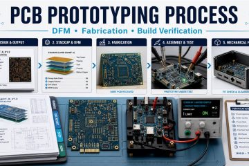
PCB Prototyping Process: DFM, Fabrication and Build Verification
Follow the PCB prototyping process from design objectives and DFM through fabrication, assembly, bring-up, verification and revision release.



Follow the PCB prototyping process from design objectives and DFM through fabrication, assembly, bring-up, verification and revision release.
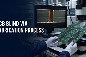
See how PCB blind vias are planned, drilled, desmeared, plated and tested—and what stack-up, DFM and supplier evidence to verify before production.
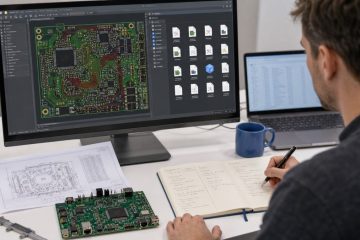
Learn how to identify and open PCB files safely, choose the right CAD or Gerber viewer, and verify layers, drills, units and revisions before manufacture.
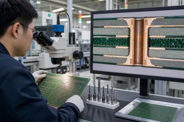
Learn how PCB vias are designed, drilled, desmeared and copper plated, how via treatments differ, and which DFM files and inspection checks prove quality.
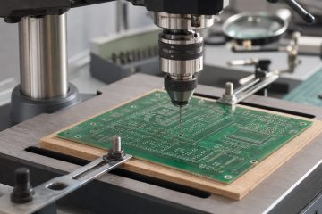
Learn how to choose PCB drill bits, set up the board, drill clean holes, inspect defects and prepare drill data for reliable PCB fabrication.
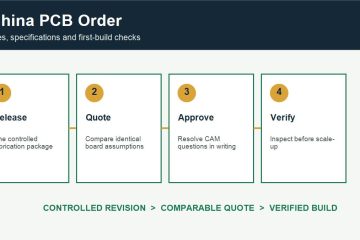
Prepare a China PCB order with practical checks for fabrication files, board specifications, quote assumptions, CAM questions and first-build inspection.

Source a China hard gold PCB with practical checks for selective plating, gold fingers, drawings, inspection and comparable RFQs.
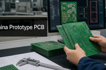
Plan a China prototype PCB order with practical DFM, file, specification, testing and first-build quote checks before production.
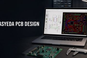
Learn how to use EasyEDA for PCB design from schematic and footprint checks through layout, DRC, Gerber export and manufacturing review.
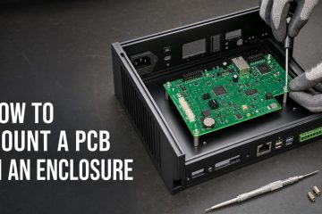
Learn how to mount a PCB in an enclosure using standoffs or rails, with clearance, grounding, thermal, vibration and DFM checks.
If you have any enquiry about quotation or cooperation, please feel free to email us at [email protected] or use the following enquiry form. Oursales representative will contact you within 24 hours. Thank you for your interest in our products.