




When RF engineers talk about “high frequency PCB,” they’re usually talking about boards that carry signals above 500 MHz — often well into the tens of gigahertz. At those frequencies, every design choice matters: the laminate, the copper surface roughness, the via placement, even the solder mask formulation. A board that works fine at 100 MHz can fall apart at 28 GHz.
This guide covers what high frequency PCBs actually are, how they differ from standard and high speed boards, which materials make sense for different frequency ranges, the design rules that keep signals clean, and what to watch out for during manufacturing.
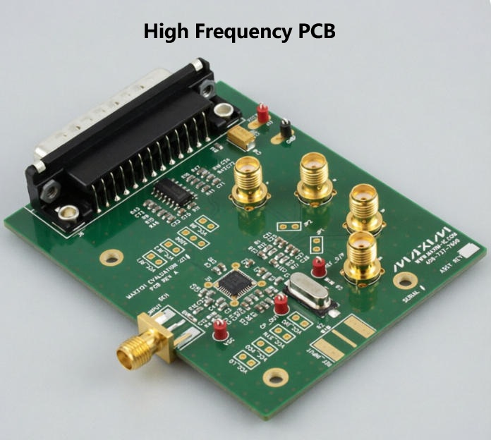
What Is a High Frequency PCB?
A high frequency PCB is a printed circuit board designed to carry signals in the radio frequency and microwave ranges — generally starting around 500 MHz and extending upward through 5G millimeter wave bands at 24–40 GHz, automotive radar at 77 GHz, and satellite communications beyond 100 GHz.
At these frequencies, the board itself becomes part of the circuit. The dielectric constant (Dk) of the substrate, the dissipation factor (Df), copper roughness, and layer stackup all directly affect signal behavior. You can’t treat the PCB as a passive carrier the way you would at lower speeds. It has to be engineered just like the components sitting on top of it.
This is what separates high frequency PCBs from regular FR4 boards: the material selection, the tolerances, and the design approach are fundamentally different.
High Frequency PCB vs Standard PCB vs High Speed PCB
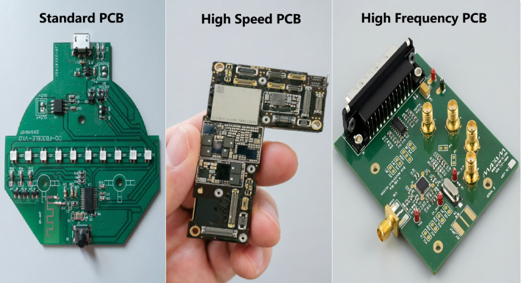
People often confuse these three categories. They overlap in some areas, but the design priorities are different.
| Aspect | Standard PCB | High Speed PCB | High Frequency PCB |
|---|---|---|---|
| Typical frequency range | DC – 100 MHz | 100 MHz – 10+ GHz | 500 MHz – 100+ GHz |
| Primary concern | Cost, basic functionality | Signal integrity, timing | Signal loss, impedance accuracy, phase stability |
| Common substrate | FR4 (1.4–1.6 Dk) | Low-loss FR4, mid-tier laminates | Rogers, PTFE, ceramic-filled laminates |
| Dk tolerance | ±0.2–0.5 | ±0.1–0.2 | ±0.05 or tighter |
| Df target | 0.02 | 0.005–0.01 | 0.001–0.004 |
| Impedance control | Not always required | Usually required | Strictly required |
| Copper surface | Standard ED copper | Low-profile copper | Ultra-low-profile or rolled annealed copper |
| Typical applications | Consumer electronics, basic controllers | Server boards, DDR interfaces, USB/HDMI | RF front ends, antennas, radar, 5G base stations |
The key difference: high speed boards focus on keeping fast digital signals intact (timing, jitter, crosstalk). High frequency boards focus on keeping analog RF signals intact (loss, phase, standing wave behavior). Many 5G and microwave designs need both, which is where material selection gets tricky.
Why Material Selection Is Everything in High Frequency PCB Design
At low frequencies, FR4 works fine for most things. At high frequencies, FR4 becomes a problem.
Here’s why. FR4 has a dissipation factor around 0.02 at 1 GHz. That number sounds small, but at 10 GHz, signal attenuation through FR4 can exceed 3–5 dB per inch depending on the build. At 28 GHz, it gets worse. For a radar module or a 5G antenna feed that needs to preserve every fraction of a decibel, FR4 simply can’t keep up.
High frequency laminates solve this by offering:
- Lower Dk (typically 2.2–3.5 instead of FR4’s 4.2–4.7), which reduces capacitive loading and speeds up signal propagation
- Tighter Dk tolerance (±0.03–0.05 vs FR4’s ±0.2–0.5), which gives more predictable impedance
- Lower Df (0.001–0.004), which directly reduces dielectric loss
- Better thermal and dimensional stability, which keeps the board’s electrical properties consistent across temperature
Common High Frequency Laminates
| Material | Dk (typical) | Df (typical) | Frequency sweet spot | Common use cases |
|---|---|---|---|---|
| Rogers RO4003C | 3.38 | 0.0027 | Up to ~30 GHz | 5G infrastructure, antennas, RF modules |
| Rogers RO4350B | 3.48 | 0.0037 | Up to ~30 GHz | Power amplifiers, filters, base station PCBs |
| Rogers RO3003 | 3.0 | 0.0013 | Up to 77+ GHz | Automotive radar, millimeter wave |
| Rogers RO3006 | 6.15 | 0.002 | Up to 30 GHz | Compact antenna designs, high-Dk applications |
| Rogers RT/Duroid 5880 | 2.2 | 0.0009 | Up to 100+ GHz | Microwave systems, military radar, satellite |
| Taconic TLC/TLY | 2.1–2.9 | 0.0008–0.0013 | Up to 77+ GHz | Automotive radar, aerospace |
| Panasonic Megtron 6 | 3.4 | 0.002 | Up to 25 GHz | High-speed digital with moderate RF |
| Isola I-Speed | 3.45 | 0.008 | Up to 10 GHz | Mid-range mixed-signal designs |
| PTFE (Teflon) | 2.1 | 0.001 | Wideband microwave | Specialty RF, military, test equipment |
| FR4 (for reference) | 4.4 | 0.02 | Below ~3 GHz | General purpose, low-cost |
A few practical notes on material selection:
- RO4003C and RO4350B are the workhorses of 5G sub-6 GHz infrastructure. They process similarly to FR4 (standard lamination cycles, compatible with lead-free soldering), which keeps manufacturing costs reasonable.
- RO3003 is a popular pick for 77 GHz automotive radar because of its extremely low loss and stable Dk across frequency.
- RT/Duroid 5880 offers the best electrical performance of anything on this list, but it’s softer, harder to drill, and significantly more expensive. You choose it when nothing else will meet the spec.
- PTFE-based materials require special handling: no chemical plasma etching, controlled drilling parameters, and sometimes proprietary surface preparation. Make sure your fab house actually has experience processing them.
Understanding Dk and Df: What They Actually Mean for Your Board
Two numbers come up constantly in high frequency PCB discussions: Dk (dielectric constant) and Df (dissipation factor). Here’s what they mean in practical terms.
Dielectric Constant (Dk)
Dk measures how much the substrate stores electrical energy in an electric field. A lower Dk means signals propagate faster through the board and experience less capacitive loading.
For a 50-ohm controlled impedance trace, Dk directly affects the required trace width for a given substrate thickness. If the Dk shifts unexpectedly — because the manufacturer used a different material batch, or the laminate absorbed moisture — the impedance shifts with it. At low frequencies, nobody notices. At 28 GHz, a few percent of impedance deviation can cause measurable reflection and signal degradation.
What to watch for:
- Dk is not constant. It varies with frequency. A material rated at Dk 3.38 at 1 GHz might be closer to 3.30 at 10 GHz. Always check the data sheet at your actual operating frequency.
- Moisture absorption affects Dk. PTFE laminates absorb very little water. Some FR4 variants absorb significantly more, which can shift Dk after the board sits in a humid environment.
Dissipation Factor (Df)
Df measures how much signal energy gets converted into heat in the substrate. Higher Df means more loss. For a long RF trace feeding an antenna, loss through the dielectric can directly reduce your link budget.
Quick example: a 2-inch microstrip trace on FR4 (Df ≈ 0.02) at 28 GHz might lose 6–8 dB. The same trace on RO3003 (Df ≈ 0.0013) might lose less than 1 dB. That’s the difference between a working 5G link and a dead one.
Practical takeaway: When you’re selecting laminate, don’t just compare Dk numbers. Pay equal attention to Df, especially if your design operates above 6 GHz.
High Frequency PCB Design Guidelines
Good high frequency PCB design starts before you open your EDA tool. Material choice, stackup planning, and understanding your loss budget come first. After that, the layout rules below help you avoid the most common pitfalls.
1. Choose the Right Material for Your Frequency
This sounds obvious, but it’s the most common mistake: designers pick FR4 to save cost, then wonder why the board doesn’t meet RF performance requirements.
General guidance:
- Below 3 GHz with modest loss requirements: high-quality FR4 (like Isola 370HR) may work
- 3–15 GHz: mid-tier laminates like RO4350B or Megtron 6
- 15–40 GHz: RO4003C, RO3003, or equivalent
- Above 40 GHz: RT/Duroid 5880, Taconic TLY, or other ultra-low-loss substrates
Don’t over-specify either. Putting RT/Duroid 5880 on a board that only carries a 1 GHz control signal wastes money. Use hybrid stackups: high frequency laminate on the RF layers, FR4 on the digital/power layers.
2. Plan Your Stackup Early
The stackup is the single most important high frequency PCB design decision. It determines impedance, loss, crosstalk, shielding, and thermal behavior.
General stackup principles for high frequency:
- Put the RF signal layer directly adjacent to a ground reference plane. This gives you a controlled return path and predictable impedance.
- Keep RF layers away from power planes when possible to reduce coupling.
- Use ground stitching vias near RF traces to create a pseudo-coaxial shielding structure.
- For hybrid builds (high frequency laminate + FR4), place the high frequency material on the outer layers where RF signals route, and use FR4 as the inner core for cost savings.
Example: 4-layer hybrid stackup for a 5G RF module
| Layer | Function | Material | Thickness (approx.) |
|---|---|---|---|
| L1 | RF signal traces | Rogers RO4003C | 8 mil |
| Prepreg | Bonding layer | RO4450F | 4 mil |
| L2 | Ground plane | FR4 (core) | 14 mil |
| L3 | Power / digital routing | FR4 (core) | 14 mil |
| Prepreg | Bonding layer | RO4450F | 4 mil |
| L4 | RF / digital traces | Rogers RO4003C | 8 mil |
This kind of hybrid stackup gives you high frequency performance on the outer layers while keeping cost under control.
3. Control Impedance Precisely
Impedance control isn’t optional at high frequencies. It’s mandatory.
For a 50-ohm microstrip or stripline, the target impedance depends on trace width, dielectric thickness, Dk, and copper thickness. At high frequencies, even small dimensional variations matter.
Key practices:
- Provide your fabricator with the exact target impedance and tolerance (typically ±10% for RF, ±5% for critical applications).
- Use your fab house’s impedance calculator or their stackup recommendation rather than relying solely on your own tool. They know the actual material properties and process capabilities of their lamination line.
- Account for copper etch trapezoidal profile. The actual trace cross-section is not perfectly rectangular, and that affects impedance. At very fine geometries, this can shift impedance by 2–3 ohms.
4. Minimize Conductor Loss
At high frequencies, current flows on the surface of the copper trace (skin effect). The rougher the copper surface, the longer the current path, and the higher the loss.
What this means in practice:
- Standard electro-deposited (ED) copper has a rough surface that adds significant loss above 10 GHz.
- Low-profile copper (like Rogers’ rolled annealed copper or treated low-profile ED copper) reduces this loss.
- If you’re building a board for 28 GHz or above, specifying the copper type matters as much as the laminate choice.
Some manufacturers offer reverse-treated copper foil (RTF) or very-low-profile (VLP) copper as options. Ask about them.
5. Route RF Traces Carefully
How you route high frequency traces on the board directly impacts signal quality.
Rules that matter:
- Keep RF traces short. Every millimeter of trace adds loss. Place RF components as close together as the thermal and layout constraints allow.
- Avoid right-angle bends. Use curved traces or 45-degree bends. At microwave frequencies, a 90-degree corner creates a capacitive discontinuity that causes reflection.
- Maintain consistent trace geometry. Don’t change trace width unnecessarily along an RF path. Width changes create impedance discontinuities.
- Keep RF traces away from digital routing. Digital signals have fast edges that couple noise into sensitive analog circuits.
- Use ground coplanar waveguide (GCPW) or microstrip with ground for most RF routing. For the highest-performance designs, buried stripline provides better shielding.
- Avoid stubs. A stub (an unterminated branch off the main RF path) creates resonance and can cause deep notches in your frequency response.
6. Get the Via Design Right
Vias are a hidden source of problems at high frequencies. A via that looks like a simple connection on a schematic is actually a three-dimensional structure with inductance, capacitance, and resonance behavior.
Practical via guidelines:
- Use ground stitching vias liberally around RF traces and near component pads.
- Keep via barrel diameter small to reduce inductive discontinuity.
- For blind or buried vias on high frequency layers, verify that the process doesn’t introduce voids or resin smear that could affect the connection.
- At millimeter wave frequencies, even the via annular ring size and anti-pad diameter affect the signal. Some designers simulate the via transition in 3D before committing to a design.
7. Don’t Ignore the Surface Finish
Surface finish affects both solderability and high frequency performance. At microwave frequencies, the surface finish on exposed RF traces (like antenna feeds or connector transitions) changes the effective conductivity.
Common options and their impact:
| Surface Finish | High Frequency Impact | Cost | Best for |
|---|---|---|---|
| ENIG | Good, smooth surface, consistent | Moderate | General RF, SMT components |
| ENEPIG | Excellent, very smooth, low loss | Higher | High-reliability RF |
| Immersion Silver | Very good, low loss, flat surface | Moderate | Broadband RF, antenna boards |
| Hard Gold | Good for connector edges, durable | Higher | Edge connectors, repeated mating |
| HASL (lead-free) | Uneven surface, not ideal for RF | Low | Avoid on RF-critical traces |
| OSP | Smooth but limited shelf life | Low | Short-term use, cost-sensitive |
For most high frequency applications, ENIG or immersion silver gives a good balance of performance and cost. Avoid HASL on any trace that carries an RF signal — the uneven surface geometry creates unpredictable loss.
8. Consider Thermal Management
High frequency power amplifiers and transmitters generate heat. If that heat doesn’t dissipate properly, the board’s Dk shifts, components drift out of spec, and reliability drops.
Thermal strategies for high frequency PCBs:
- Use thermal vias under power amplifier pads to pull heat to an internal ground plane or a metal core.
- Consider metal-core or IMS (insulated metal substrate) builds for very high power RF designs.
- Route heat away from temperature-sensitive RF circuits (oscillators, PLLs, low-noise amplifiers).
- If using PTFE laminates, be aware they have lower thermal conductivity than FR4. Plan accordingly.
9. Account for Manufacturing Tolerances
High frequency designs are less forgiving of manufacturing variation. Before finalizing your design, talk to your fabricator about their capabilities.
Key questions to ask:
- What is your minimum trace width and spacing for RF layers?
- What impedance tolerance can you guarantee?
- Do you have experience processing Rogers, PTFE, or other high frequency laminates?
- What copper foil types are available?
- Can you provide VNA or TDR test data for impedance verification?
- What is your via fill capability for ground stitching vias?
Not every PCB manufacturer can reliably build high frequency boards. A fab house that does great work on standard FR4 might struggle with hybrid stackups or PTFE processing. Verify their experience before committing to a supplier.
Common High Frequency PCB Applications
High frequency PCBs show up across several industries, each with its own performance requirements.
5G Telecommunications
5G NR (New Radio) uses both sub-6 GHz and millimeter wave bands. Base station boards, radio units, and antenna arrays all require high frequency laminates with low loss and tight impedance control. For massive MIMO systems, the number of RF channels per board has increased dramatically, making laminate cost and manufacturability critical.
Automotive Radar
77 GHz (and 79 GHz) automotive radar for ADAS and autonomous driving is one of the fastest-growing high frequency PCB applications. These boards need extremely low loss, stable Dk across temperature (-40°C to +125°C), and tight dimensional tolerances. Materials like RO3003 and Taconic TLY are common choices.
Satellite and Aerospace Communication
Satellite communications (both ground stations and space-borne payloads) operate across wide frequency ranges, from L-band up to Ka-band and beyond. These systems often require the best-performing laminates available, along with qualification to military or aerospace standards.
RF and Microwave Test Equipment
Test and measurement instruments — network analyzers, spectrum analyzers, signal generators — need boards with extremely predictable, low-loss performance. RT/Duroid 5880 and similar ultra-low-loss materials are standard in this space.
Medical and Industrial RF
Applications like microwave ablation systems, industrial RF heating, and RFID readers also require high frequency PCBs, though often at more moderate frequencies and with different cost constraints than telecom or automotive.
How to Evaluate a High Frequency PCB Manufacturer
Choosing the right manufacturer matters as much as the design itself. Here’s what to look for:
Material capability:
- Stock or approved sourcing for Rogers, Taconic, Panasonic, and other high frequency laminates
- Experience with hybrid stackups (high frequency + FR4)
- Ability to process PTFE and other sensitive materials
Process capability:
- Controlled impedance with documented tolerance
- Fine line/space capability (if your design requires it)
- Via fill and via-in-pad options
- Multiple surface finish options including ENIG, ENEPIG, and immersion silver
Testing and quality:
- VNA (vector network analyzer) testing for high frequency performance verification
- TDR (time domain reflectometry) for impedance measurement
- Cross-section analysis capability
- IPC Class 2 or Class 3 manufacturing standards
- ISO 9001 or equivalent quality system
Documentation:
- Stackup confirmation with actual material properties
- Impedance test reports
- Certificate of compliance for materials used
A manufacturer that checks these boxes can save you from expensive redesigns and failed prototypes.
High Frequency PCB Checklist
Before sending your design to fabrication, run through this list:
- Laminate material selected and specified by part number (not just “high frequency material”)
- Dk and Df values verified at your operating frequency from the material data sheet
- Stackup designed with ground reference plane adjacent to every RF signal layer
- Impedance targets defined with tolerance
- Copper foil type specified (standard ED, low-profile, or rolled annealed)
- RF traces kept short, with smooth bends and consistent width
- Ground stitching vias placed around RF traces and component pads
- No stubs or unterminated branches on RF signal paths
- Digital and RF routing adequately separated
- Surface finish appropriate for RF traces (ENIG or immersion silver preferred, no HASL on RF paths)
- Thermal management addressed for power-dissipating components
- Manufacturing tolerances reviewed with the fabricator
- Fab house confirmed to have experience with your specified materials
- Impedance test and RF test requirements communicated to the manufacturer
FAQ
What is considered high frequency in PCB design?
There’s no single hard cutoff, but most engineers consider PCB signals above 500 MHz to be in the “high frequency” range. As frequencies increase into the multi-GHz range (5G, radar, satellite), the requirements for materials, design, and manufacturing become significantly more demanding.
What is the difference between high frequency and high speed PCB?
High speed PCBs focus on maintaining signal integrity for fast digital signals — think DDR memory interfaces, PCIe lanes, or USB 3.0 traces. The concerns are timing, jitter, and crosstalk. High frequency PCBs deal with analog RF and microwave signals where the primary concerns are signal loss, impedance accuracy, and phase stability. Many advanced designs involve both high speed digital and high frequency analog on the same board.
Can FR4 be used for high frequency applications?
Standard FR4 is generally not suitable for frequencies above 3–5 GHz due to its high dielectric loss. However, there are enhanced FR4 variants (like Isola I-Speed or Panasonic Megtron 6) that push the usable range higher. For serious RF work above 10 GHz, purpose-built high frequency laminates are almost always necessary.
What is the best material for high frequency PCB?
There’s no single “best” material — it depends on your frequency, loss budget, and cost constraints. Rogers RO4003C and RO4350B are widely used workhorses for 5G and general RF up to about 30 GHz. For millimeter wave (above 30 GHz), RO3003, RT/Duroid 5880, or Taconic TLY are common choices. The right material is the one that meets your electrical requirements at the lowest practical cost.
How does Dk affect PCB performance?
Dielectric constant determines signal propagation speed and the physical dimensions needed for impedance control. A higher Dk means slower signal speed and narrower trace widths for a given impedance. Dk variation across frequency or temperature causes impedance shifts, which lead to reflections and signal degradation at high frequencies.
Why is copper surface roughness important for high frequency PCBs?
At high frequencies, the skin effect forces current to flow on the surface of the copper trace. Rough copper increases the effective path length of the current, which raises conductor loss. At frequencies above 10 GHz, copper roughness can contribute as much loss as the dielectric itself. Specifying low-profile copper foil is one of the most cost-effective ways to improve high frequency performance.
What surface finish is best for high frequency PCBs?
ENIG (Electroless Nickel Immersion Gold) and immersion silver are the most common choices for RF-critical traces. Both provide a smooth, flat surface with predictable electrical properties. Avoid HASL on RF signal paths because the uneven surface creates inconsistent loss. For the highest performance, ENEPIG offers an excellent combination of smoothness and solderability.
How many layers does a high frequency PCB need?
Layer count depends on the design complexity, not the frequency. Simple RF circuits might work on 2 or 4 layers. Complex 5G or radar modules with multiple RF channels, power distribution, and digital control might need 6, 8, or more layers. The key rule is that every RF signal layer should be adjacent to a solid ground reference plane.
Getting Started with Your High Frequency PCB Project
Whether you’re designing a 5G RF module, a 77 GHz radar board, or a satellite communication system, getting the material, stackup, and design rules right from the start saves time and money down the line.
If you’re unsure about material selection, stackup planning, or whether your design is ready for manufacturing, it helps to work with a PCB manufacturer that has hands-on experience with high frequency laminates and can provide engineering feedback before you commit to a prototype build.



0 Comments