




What Is a PCB Substrate?
A PCB substrate is the insulating material that gives a printed circuit board its mechanical structure and helps control its electrical and thermal behavior. Copper traces carry the current and signals; the substrate supports those traces, separates copper layers, and affects how the finished board responds to heat, voltage, vibration, moisture, and high-frequency signals.
In everyday conversation, people often use PCB substrate to mean the board material as a whole. In a fabrication drawing, however, that wording may be too vague. A multilayer PCB is normally built from copper-clad cores and bonding sheets called prepreg. The material family, resin system, glass style, cured thickness, copper weight, and construction all matter.
This distinction is practical, not academic. If a drawing says only “FR-4, 1.6 mm,” the factory still has to resolve the exact laminate system, individual dielectric thicknesses, copper construction, finished thickness tolerance, and any controlled-impedance requirements. Those choices can change manufacturability and the electrical result.
Are Substrate, Laminate, Core and Prepreg the Same?
No. These words describe related materials, but they are not interchangeable in a production stackup.
| Term | Plain-language meaning | Typical role | What to verify |
|---|---|---|---|
| Substrate | A general name for the insulating base material | Describes the material platform or board base | Whether the document means a material family or a specific construction |
| Laminate | A cured sheet made from reinforcement and resin, often with copper foil bonded to it | Used to make cores or copper-clad laminate | Grade, thickness, copper weight, datasheet revision, and test method |
| Core | A rigid, fully cured dielectric sheet, commonly copper-clad on one or both sides | Forms a stable part of a multilayer stackup | Cured dielectric thickness and copper construction |
| Prepreg | Glass reinforcement impregnated with partially cured resin | Flows and cures during lamination to bond layers together | Glass style, resin content, pressed thickness, and fill requirements |
| Dielectric | Any insulating layer between conductors | Provides electrical separation and influences impedance | Actual thickness, dielectric constant, and applicable frequency |
A useful mental model is that a core is already cured, while prepreg becomes the bonding dielectric during lamination. Prepreg does not keep the same nominal thickness after pressing. Resin moves around copper features and fills spaces, so its final thickness depends on glass style, resin content, adjacent copper pattern, pressure, and the fabricator’s qualified process.
This is why a material name alone is not a complete stackup. For a deeper comparison of commonly available families, see our PCB board material selection guide.
Where Does the Substrate Sit in a PCB Stackup?
The substrate is not one single slab hidden under the copper. In a multilayer board, insulating material appears between every conductive layer. Some dielectric layers are cores; others are cured prepreg. Together with the copper foils, they form the finished stackup.
Consider a simple four-layer construction. The outer copper layers may begin as foil, the inner signal and plane layers may be etched on a copper-clad core, and prepreg may bond the outer foils to that core during lamination. The exact construction varies by fabricator, material system, finished thickness, copper weight, and impedance target.
That variation has consequences. A 0.20 mm dielectric between a signal and reference plane does not behave like a 0.10 mm dielectric. If controlled impedance matters, trace geometry and the finished dielectric structure must be solved together. Do not lock a trace width from a generic online calculator and then ask the factory to make any convenient stackup around it.
Which Substrate Properties Actually Change Board Performance?
The useful properties depend on the job the board must do. A motor-control board, a 10 GHz RF board, a wearable flex circuit, and a power LED board do not fail for the same reasons. Start with the design risk, then choose the properties that control that risk.
| Property | What it describes | Why it matters | Common mistake |
|---|---|---|---|
| Dk / dielectric constant | How the material stores electric-field energy | Influences impedance, wavelength, and propagation delay | Treating one datasheet Dk value as valid for every frequency and test method |
| Df / dissipation factor | A measure related to dielectric energy loss | Contributes to insertion loss, especially as frequency and route length rise | Choosing “low loss” without a channel loss budget |
| Tg | The glass-transition region of the cured resin system | Indicates a change in mechanical behavior and expansion rate | Using Tg alone as a complete reliability rating |
| Td | Thermal decomposition behavior under a stated test condition | Helps assess resistance to severe thermal exposure | Assuming Td equals a safe continuous operating temperature |
| CTE | How much the material expands with temperature | Affects plated-hole, via, component, and dimensional reliability | Ignoring the axis, temperature range, and test condition |
| Thermal conductivity | How readily heat moves through the material | Influences the thermal resistance of the heat path | Comparing conductivity without considering thickness and area |
| Moisture absorption | How much moisture the material takes up under a stated test | Can affect processing, insulation behavior, and dimensional stability | Comparing values measured with different methods |
| Flammability classification | How a tested specimen behaves in a specified flame test | May be required by the end product or certification plan | Reading UL 94 V-0 as “the material cannot burn” |
The pattern is important: every number needs context. Ask which grade was tested, by which method, at what frequency or temperature, in which direction, and at what specimen thickness. Two values with different methods may not be a fair comparison.
When Is Standard FR-4 the Right Baseline?
Standard FR-4 is a sensible starting point for many rigid digital, analog, control, and general industrial boards when the design does not have unusually severe thermal, loss, voltage, or dimensional demands. FR-4 is a material class, not one universal recipe. Different suppliers and grades can have different resin systems and measured properties.
Use FR-4 as the baseline when the fabricator can meet the required layer count, thickness, copper, hole structure, assembly profile, operating environment, and electrical performance with a qualified material system. Then state the performance requirements that matter instead of casually naming a premium grade.
For example, a moderate-speed four-layer controller may not benefit from an expensive low-loss laminate. Its more important controls could be a stable stackup, continuous reference planes, suitable creepage and clearance, sensible via design, and an assembly-compatible Tg. Our guide to FR-4 substrate material explains the basic construction and terminology in more detail.
Why Are High-Tg and Low-Loss Laminates Not the Same Upgrade?
High-Tg and low-loss materials solve different primary problems. A higher Tg addresses the temperature range in which the resin system changes mechanical behavior. A low-loss laminate is formulated and characterized to reduce electrical loss and provide more predictable high-frequency performance. One label does not guarantee the other.
Suppose a board suffers plated-through-hole stress during repeated lead-free assembly. The investigation should include z-axis expansion, Td, time above Tg, board thickness, copper distribution, hole geometry, bake and storage conditions, and the actual reflow profile. Simply ordering “low-loss material” would not directly solve that failure mode.
Now suppose a long RF route exceeds its insertion-loss budget. Raising Tg alone may not materially improve the channel. The design team instead needs a dielectric system with appropriate Dk/Df data, a controlled stackup, copper roughness assumptions, trace geometry, connector and via-transition models, and a verification plan.
How Do Polyimide, Metal-Core and Ceramic Substrates Differ?
They differ in construction and in the problem each platform is best positioned to solve. Polyimide-based flex constructions enable bending and compact interconnects. Metal-core boards create a short heat-spreading path through a dielectric to an aluminum or copper base. Ceramic substrates offer electrical insulation with much higher thermal conductivity than ordinary organic laminates, but bring different cost, brittleness, processing, and design constraints.
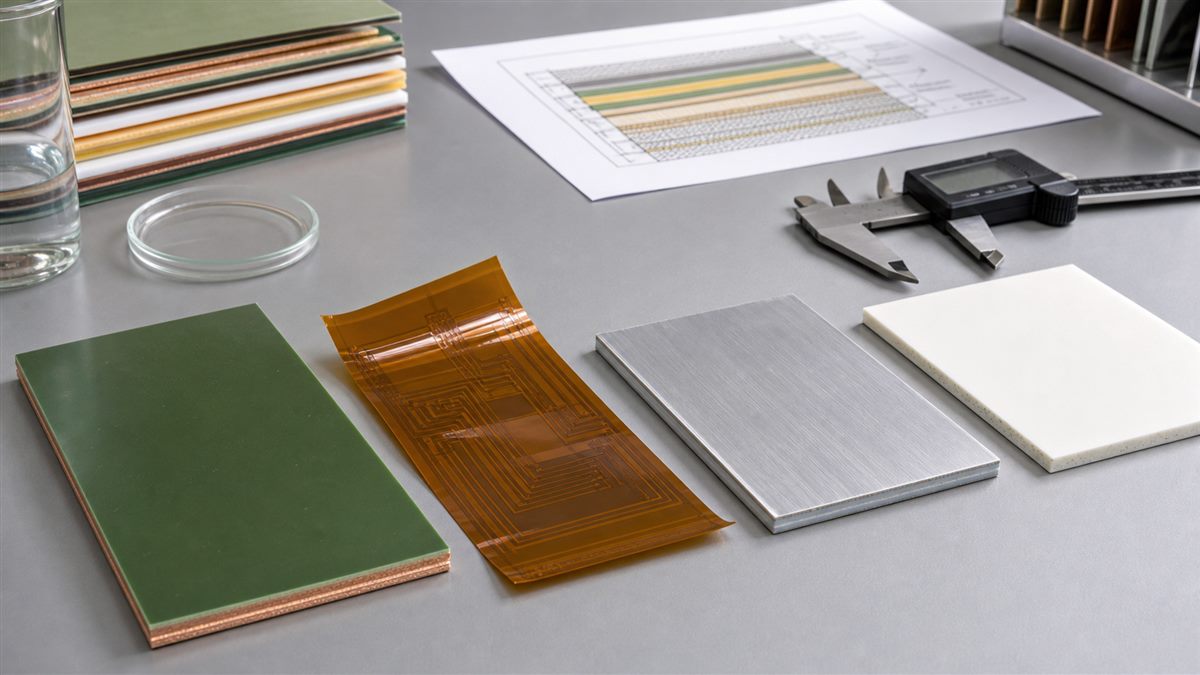
| Platform | Useful when | Main design question | Important caution |
|---|---|---|---|
| Rigid FR-4 family | General rigid circuitry and multilayer interconnect | Can the selected grade meet thermal, electrical and reliability needs? | “FR-4” alone does not identify one exact material |
| Polyimide flex | Dynamic or installation bending, compact cable replacement | Where are the bend zones, neutral axis and stiffener transitions? | Rigid-board trace and via rules cannot be copied blindly |
| Metal-core | Heat-generating devices needing a short path to a metal base | What is the total junction-to-coolant thermal path? | The dielectric layer may dominate thermal resistance |
| Ceramic | High-temperature, high-power, RF or hermetic-oriented applications | Which ceramic system and metallization process fit the design? | High conductivity alone does not remove mechanical and cost constraints |
These options also lead to different supplier capabilities. Review our pages for flexible PCB manufacturing, aluminum PCB, and ceramic PCB manufacturing when the architecture points beyond conventional rigid FR-4.
How Do Dk and Df Affect Signal Integrity?
Dk affects how electromagnetic fields interact with the dielectric, so it influences impedance and propagation. Df describes dielectric loss under a stated test condition, so it contributes to signal attenuation. Neither number should be selected in isolation.
For a controlled-impedance trace, the effective electromagnetic environment includes dielectric thickness, trace width and thickness, nearby copper, solder mask, material Dk, glass weave, copper profile, and fabrication tolerances. For high-frequency loss, the route length, frequency content, conductor loss, dielectric loss, vias, connectors, and launches all contribute.
A practical workflow is:
- Define the interface, edge rate or frequency range, route length, impedance target, and loss budget.
- Choose a material family with characterized data in a relevant frequency range and ask which values the fabricator uses for field solving.
- Let the fabricator propose a manufacturable stackup using stocked materials and qualified press cycles.
- Model the actual stackup, including conductor assumptions and transitions.
- Specify impedance tolerance and, when risk warrants it, coupon and test-report requirements.
As one grade-specific example, Rogers publishes a process Dk of 3.48 ± 0.05 and a dissipation factor of 0.0037 at 10 GHz for RO4350B. Those figures are useful for that product under the stated conditions; they are not universal values for every “Rogers PCB” or every test method. See the RO4350B product data for the complete context.
How Do Tg, Td and CTE Affect Fabrication and Reliability?
Tg, Td, and CTE describe different thermal behaviors. Tg marks a transition region in the cured polymer’s mechanical response. Td concerns decomposition under a specified test. CTE describes dimensional expansion with temperature. A robust material decision considers all three alongside the actual thermal cycle and board construction.
Why does that matter? During lamination, soldering, rework, temperature cycling, and service, the PCB and its copper features expand differently. Excessive z-axis movement can strain plated holes and vias. Repeated thermal excursions can reveal weaknesses that a room-temperature inspection cannot.
When reviewing a material for a demanding assembly, ask:
- What Tg and Td methods are reported, and are we comparing like with like?
- What is the z-axis CTE below and above Tg?
- How many assembly and repair heat cycles are expected?
- What is the maximum board thickness and smallest finished hole or via?
- Are buried vias, blind vias, stacked microvias, heavy copper, or unbalanced copper involved?
- What qualification or reliability test matches the real product risk?
Do not convert a datasheet Tg directly into a maximum continuous-use temperature. Operating limits belong to the qualified material, board construction, assembly, enclosure, components, and end-product certification together.
Why Does Thermal Conductivity Not Tell the Whole Cooling Story?
Thermal conductivity is only one part of the heat path. The approximate one-dimensional thermal resistance of a uniform layer is:
Rth = t / (k × A)
where t is thickness, k is thermal conductivity, and A is the effective heat-flow area. A thin dielectric with modest conductivity can sometimes create less resistance than a much thicker layer with a higher conductivity. Real boards also spread heat in three dimensions, so copper area, thermal vias, interfaces, component attachment, airflow, heatsinks, and enclosure contact all matter.
For a simple comparison, if two layers have the same area but Layer B is twice as thick and twice as conductive as Layer A, their ideal one-dimensional thermal resistance is equal. Looking only at the larger conductivity number would give the wrong decision.
Ceramic data illustrates how large grade differences can be. CeramTec lists thermal conductivity of at least 170 W/mK at 20°C for one AlN HP material grade. That is a material-specific value, not a promise for every ceramic board or for the complete component-to-ambient path. Use the manufacturer’s aluminum nitride material information as a starting point, then analyze the full assembly.
How Should You Compare PCB Material Datasheets?
Compare datasheets by property, condition, method, direction, and grade—not by copying the boldest number from each page. Before building a comparison table, make sure the values describe the same thing.
- Fix the application requirement. Write the real constraint: impedance, loss, thermal path, bending, voltage, assembly cycles, operating environment, or certification.
- Record the exact product and revision. A family name is not enough.
- Match test methods and conditions. For Dk/Df, check frequency and method. For CTE, check axis and temperature range. For moisture, check conditioning and method.
- Separate typical from guaranteed values. A typical number helps design exploration but may not be a procurement limit.
- Check available constructions. Confirm core thicknesses, prepreg styles, copper options, panel availability, and lead time with the fabricator.
- Ask how fabrication changes the result. Pressed prepreg thickness, resin fill, copper roughness, etching, and tolerance affect the finished board.
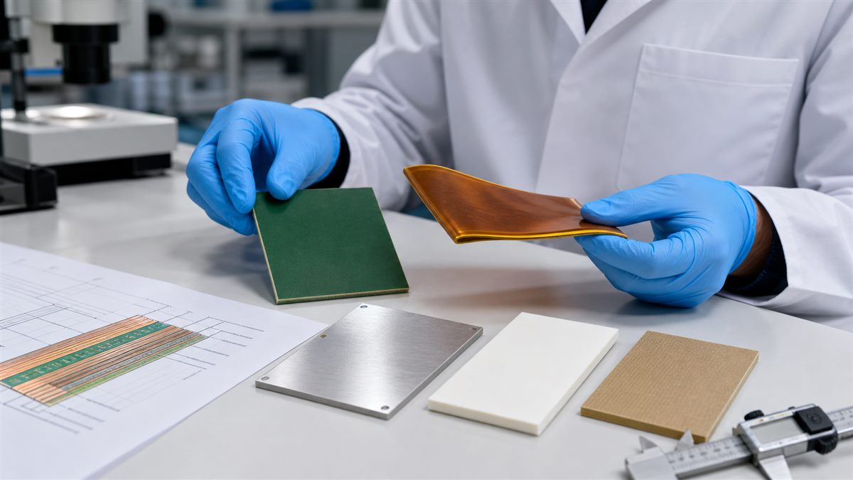
For laminate and prepreg procurement language, IPC-4101 covers specification requirements for base materials used in rigid and multilayer PCBs, while IPC-4103 addresses high-speed/high-frequency applications. The slash sheet or material designation is part of the conversation, but it does not replace a complete stackup and performance requirement.
How Do You Match a Substrate to the Application?
Match the substrate to the dominant failure risk, then check that the choice does not create a new manufacturing problem. The table below is a screening tool, not a final material approval.
| Application condition | Start by checking | Likely material direction | Evidence needed before release |
|---|---|---|---|
| General controller or interface board | Layer count, assembly profile, environment, voltage | Qualified FR-4 system | Fabricator stackup and material declaration |
| Long high-speed serial channels | Loss budget, impedance, route length, via transitions | Low-loss laminate where analysis justifies it | Stackup model, field-solver values, coupon/test plan |
| RF or microwave circuit | Frequency, insertion loss, phase stability, launch design | Characterized RF laminate or hybrid construction | Grade-specific RF data and fabrication capability |
| High-power LED or power device | Heat source, dielectric thickness, copper spreading, cooling interface | Metal-core, heavy-copper FR-4, or ceramic depending on the path | Thermal model and interface assumptions |
| Dynamic bending | Bend radius, cycle count, layer placement, stiffeners | Polyimide flex construction | Bend-zone rules and mechanical drawing |
| Repeated severe thermal cycles | CTE, via structure, board thickness, reflow and service range | Thermally robust qualified laminate system | Reliability plan tied to the actual construction |
Do not begin with “Which material is best?” Begin with “What must the board survive, and what result must we verify?” That wording turns a catalog search into an engineering decision.
What Should the Stackup and Fabrication Notes Specify?
A usable fabrication package defines the required result while leaving room for the fabricator to use a qualified, manufacturable construction. Over-specifying an unavailable glass style can increase lead time; under-specifying the electrical and reliability target can produce the wrong board.
Include, where applicable:
- Layer order, layer function, and finished board thickness with tolerance.
- Finished copper requirements and any special copper distribution concerns.
- Material family or approved grade list, plus the performance properties that cannot be substituted.
- Controlled-impedance nets, target impedance, tolerance, and coupon/report requirement.
- Minimum dielectric spacing that is safety- or performance-critical.
- Operating and assembly temperature conditions that affect material qualification.
- Flammability or certification requirements tied to the end product.
- Special structures such as flex zones, metal cores, cavities, sequential lamination, or ceramic metallization.
A strong note might say that equivalent material requires written approval and must meet specified Dk/Df conditions, Tg/Td/CTE limits, flammability recognition, thickness availability, and process compatibility. A weak note says only “use high-quality FR-4.” The second statement cannot be objectively verified.
What Should You Send for a PCB Substrate Review?
Send enough information for the fabricator to review the complete board, not just a material name. The fastest substrate decision usually happens when electrical, mechanical, thermal, and production constraints arrive together.
| Send this | Why the fabricator needs it |
|---|---|
| Gerber or ODB++ data and NC drill files | Reveals layer content, copper distribution, holes, clearances, and manufacturability |
| Proposed stackup or layer-function list | Shows the intended reference relationships and board construction |
| Fabrication drawing | Defines finished thickness, tolerances, finish, dimensions, special notes, and acceptance needs |
| Impedance table | Links target values and tolerances to actual layers and nets |
| Frequency, edge-rate, or loss requirement | Explains why dielectric and conductor behavior matter |
| Operating and assembly temperature profile | Supports thermal-material and reliability review |
| Thermal load and cooling concept | Prevents conductivity from being judged without the full heat path |
| Flex, vibration, voltage, moisture, or certification constraints | Identifies nonstandard risks and required evidence |
| Approved materials or substitution rules | Prevents unreviewed changes while preserving realistic supply options |
For a manufacturability and material review, send these files and constraints through the PCBtry contact page. Ask the engineering team to return the proposed production stackup, exact material designation, controlled-impedance assumptions, and any recommended change before quotation is treated as final.
PCB Substrate FAQ
Is PCB substrate the same as FR-4?
No. FR-4 is a widely used class of flame-retardant glass-reinforced epoxy laminate, while PCB substrate is the broader term. Substrates can also use polyimide, RF laminate systems, metal-core constructions, ceramics, and other materials.
Does a multilayer PCB use one substrate?
It uses one material system or sometimes a qualified hybrid system, but the physical stack normally contains multiple dielectric layers. Those layers may be cured cores and prepreg that cures during lamination.
Is higher Tg always better?
No. Higher Tg may help when thermal-mechanical exposure is the governing risk, but it does not automatically mean lower RF loss, better heat conduction, easier fabrication, or better value. Select it against the actual assembly and service conditions.
Can I specify only the dielectric constant?
Not for a production-ready controlled-impedance design. You also need the stackup, dielectric thicknesses, trace geometry, copper assumptions, impedance tolerance, relevant frequency context, and a fabricator review.
Which PCB substrate dissipates heat best?
There is no single answer without the complete heat path. Ceramic and metal-core platforms can improve specific paths, but dielectric thickness, copper spreading, thermal vias, interfaces, heatsinks, airflow, and component attachment determine the assembly result.
Can the factory substitute an equivalent laminate?
Only under a defined substitution rule. State which properties, test conditions, certifications, constructions, and electrical results must remain equivalent, and require approval when the change could affect qualification or performance.
What is the difference between an IC substrate and a PCB substrate?
An IC substrate is a high-density interconnect structure used between a semiconductor package and the larger PCB. It can resemble a very fine PCB, but its feature sizes, materials, packaging role, and manufacturing controls are different from a conventional printed circuit board.
What is the first question to ask a PCB fabricator about substrate?
Ask for the exact proposed production stackup and material designation for your files. Then verify whether it meets the electrical, thermal, mechanical, assembly, certification, availability, and substitution requirements that matter to your product.



0 Comments