




How does a PCB board work?
A printed circuit board works as a mechanical platform and an electrical interconnection system. Insulating material supports patterned copper conductors; pads connect component terminals, traces and planes carry power or signals, and plated vias connect copper on different layers. The components perform sensing, switching, computing or power conversion. The PCB gives those components the intended conductive paths and physical positions.
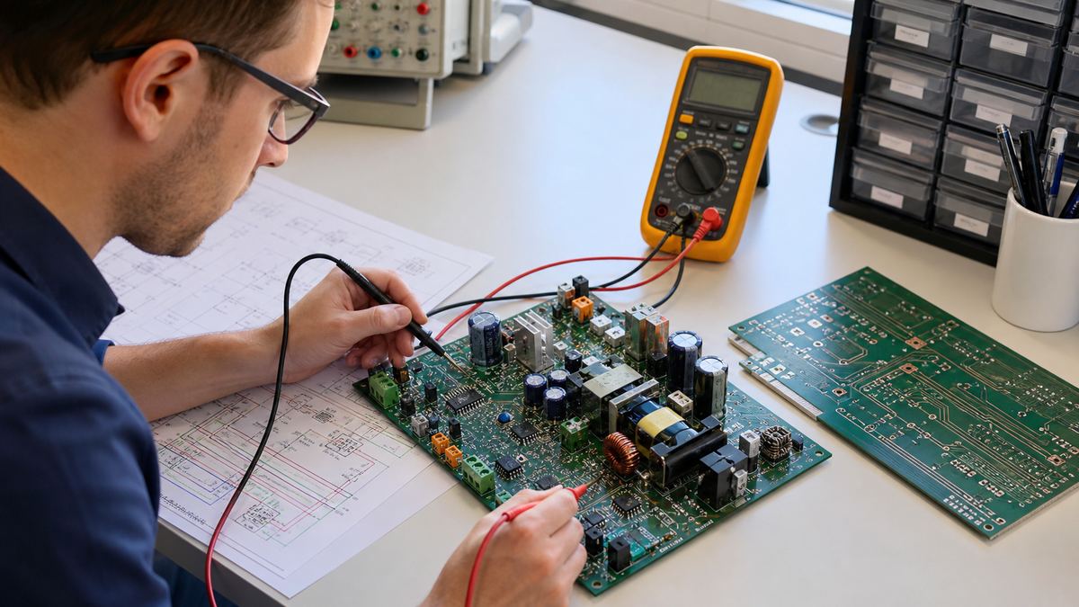
PCB and PCBA are not the same thing
A bare PCB contains laminated dielectric, copper features, holes, finish, solder mask and legend but no functional components. A PCBA is the populated assembly. A bare board can be tested for continuity and isolation, but it normally cannot perform the final product function until the specified components, firmware and external connections are present.
Understand the main PCB features
| Feature | What it does | What can go wrong |
|---|---|---|
| Trace | Connects circuit nodes | Open, excessive resistance or wrong geometry |
| Pad | Provides component/connector landing | Poor wetting, lift or insufficient size |
| Via | Connects copper layers | Barrel defect or unintended stub |
| Plane | Distributes power/ground and supports return current | Split or bottleneck |
| Dielectric | Insulates and spaces copper | Wrong thickness/material or breakdown |
| Solder mask | Protects copper and separates solderable areas | Misregistration or mask dam loss |
A circuit needs a complete current loop
Current does not simply travel from a source to one component and stop. It leaves the source, passes through loads and conductive paths, then returns to the source. For example, an LED circuit needs a supply trace, current-limiting element, LED, return trace or ground plane, and correct polarity. One open joint anywhere in the loop stops the intended current.
Components create function; copper creates connections
Resistors limit current or set voltages, capacitors store charge and filter, diodes control current direction, transistors switch or amplify, and integrated circuits implement complex functions. Copper traces do not replace these parts. The PCB translates the schematic’s electrical nodes into manufacturable physical connections.
Power and ground reach every functional block
Power enters through a connector, battery contact or regulator and is distributed to loads. Ground is a reference and return network, not a magic zero-voltage sink. Trace width, copper thickness, plane shape, via count and connector rating affect voltage drop, heat and current capacity.
Signals travel with return paths
A changing signal creates electromagnetic fields and a corresponding return current, commonly along a nearby reference plane. Discontinuous references, long detours and poor layer transitions can increase noise and interference. High-speed operation therefore depends on geometry and stackup, not only schematic connectivity.
Vias connect layers in a multilayer PCB
A plated through via forms a conductive barrel through the board; blind, buried and microvia structures connect selected layers. Signal vias may need nearby ground vias when changing reference layers. Power vias may be paralleled when one barrel cannot meet current, temperature or reliability requirements.
Layers separate routing, references and functions
Single- and double-sided boards expose limited routing surfaces. Multilayer boards add internal signal, power and ground copper with controlled dielectric spacing. More layers do not automatically improve a design; the stackup must support routing density, return paths, impedance, manufacturability and cost.
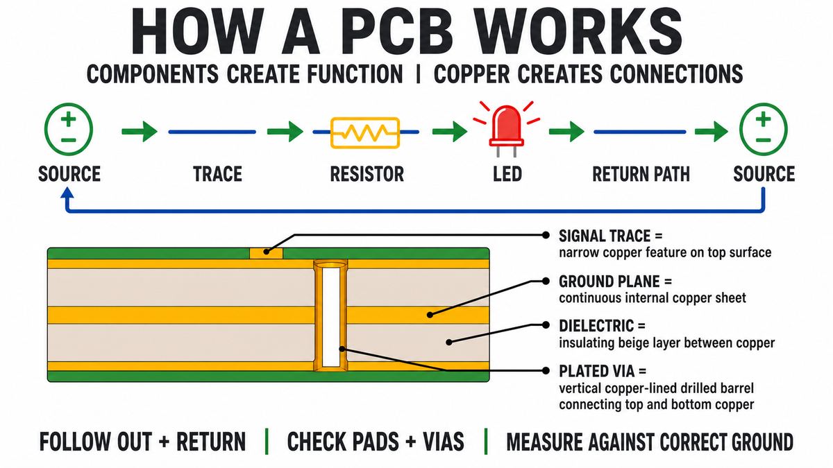
Use one LED circuit as a simple example
- A supply connector applies voltage to a power net.
- A copper trace carries current to a resistor.
- The resistor limits current before it reaches the LED.
- The LED converts electrical energy into light when oriented correctly.
- A ground trace or plane returns current to the source.
- Pads and solder joints connect each component terminal to its net.
If the LED does not light, check the whole loop: source, polarity, resistor value, trace continuity, solder joints and return path.
Solder joints connect component terminals to pads
A reliable joint wets the component termination and PCB finish, creating electrical and mechanical connection. Solder is not intended to bridge design gaps or hold a heavily loaded connector without mechanical support. Assembly drawings and inspection criteria define orientation, polarity and workmanship.
Protection layers do different jobs
Solder mask covers most outer copper but is not the main structural dielectric. Surface finish protects exposed pads and supports soldering or contact. Silkscreen identifies parts and test points but carries no current. Conformal coating, when specified, is a separate post-assembly environmental protection.
How to inspect a PCB path
- Start with the schematic net and identify source, load and return.
- Locate corresponding connector pins, component pads and test points.
- Follow visible traces and layer transitions; use layout data for hidden layers.
- With power removed, check continuity and unintended shorts where appropriate.
- With controlled power, measure voltage relative to the correct reference.
- Record the last correct node and first incorrect node.
How a PCB is manufactured from the design
Fabrication data defines copper images, drilled holes, board outline, mask and legend. The manufacturer images and etches copper, forms holes, plates interconnections, laminates layers where needed, applies finishes and tests the bare board. Assembly then adds components. A complete manufacturing request needs consistent Gerbers or ODB++, drill files, stackup and drawing.
PCB working principle FAQ
Does electricity flow through the green part of a PCB?
The green surface is usually solder mask. Current mainly flows in copper beneath or around it; the laminate and mask are insulating under normal conditions.
Why are PCB traces different widths?
Width is chosen for current, temperature rise, impedance, spacing and manufacturing needs. A power path may need more copper than a low-current control signal.
What does a ground plane do?
It provides a low-impedance reference and return path, can aid shielding and spreads current. Its effectiveness depends on continuity and stackup.
Can a PCB work without components?
A bare board can provide passive connections, but most product functions require assembled components and sometimes firmware.
Why do PCBs have multiple layers?
Layers support routing density, power/ground distribution, return paths and controlled geometry. The required count depends on the design.
What is a via?
A via is a plated connection between copper layers. Different via structures connect all or selected layers.
How does a PCB carry data?
Voltage and current changes propagate along conductive structures whose geometry and reference paths affect signal quality.
What makes a PCB fail?
Opens, shorts, poor joints, damaged components, contamination, overstress, incorrect design or unsuitable materials can interrupt intended operation.
What files explain how a PCB is connected?
The schematic shows logical connections; PCB layout data shows physical geometry; fabrication and assembly files tell suppliers how to build it.
Turn a working circuit into a manufacturable PCB
Send the schematic, fabrication data, drill files, stackup, board drawing and test requirements through the PCBTRY contact page for DFM and quotation review. Include BOM and assembly data when you need a complete PCBA rather than a bare board.



0 Comments