




What Is the HDI PCB Manufacturing Process?
The HDI PCB manufacturing process builds a multilayer board with finer conductors and smaller interconnections than a conventional through-hole board. Laser-drilled microvias, blind or buried connections, thin dielectric layers and sequential build-up cycles make it possible to escape fine-pitch packages and place more routing in less area. The same features also make registration, copper filling and thermal reliability much less forgiving.
PCBTRY supports HDI projects through stack-up review, DFM feedback, bare-board fabrication and downstream assembly coordination. For an engineering review, send the Gerber or ODB++ data, NC drill files, proposed stack-up, finished thickness, material requirements, impedance notes, quantity and test expectations to [email protected]. The useful first question is not simply whether a factory “makes HDI,” but whether it can build and verify your exact via structure.
How Does the HDI PCB Manufacturing Process Work?
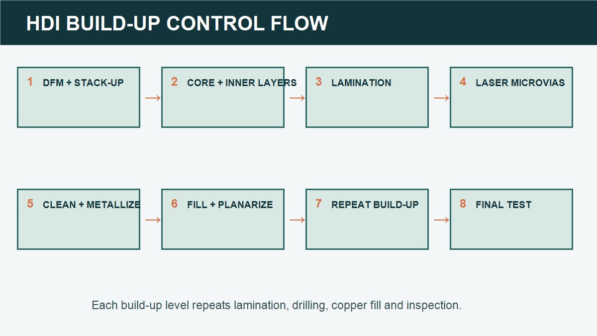
HDI fabrication is a repeated build-up loop: approve the construction, make a stable core, add a thin dielectric layer, form and metallize microvias, then repeat only as many times as the interconnect structure requires.
1. Engineering review and DFM analysis. CAM engineers compare the data set, fabrication drawing and proposed stack-up. They check microvia type, capture pads, annular features, copper balance, dielectric thickness, impedance structures and whether stacked or staggered vias are actually required. An unresolved mismatch here can change the lamination count or leave a via landing without enough registration margin.
2. Core and inner-layer fabrication. The inner core is imaged, etched and inspected before it becomes buried inside the build. Finished conductor width matters more than the artwork alone because etch compensation must account for copper thickness and process behavior. Inner-layer AOI catches opens, shorts and pattern defects before lamination makes repair impractical. See how etch compensation protects finished trace width.
3. First lamination and reference registration. Cores, prepreg or build-up dielectric and copper are laminated under a material-specific cycle. The factory must control resin movement, thickness and layer shift while preserving targets for the next drilling operation. If the reference layers move, laser vias may still look centered from the surface while missing the intended capture pad below.
4. Laser microvia drilling. A laser removes the dielectric to expose the target copper. Energy, focus, pulse strategy and material absorption affect the via profile and the condition of the landing pad. Too little removal leaves residue; too much can damage copper or enlarge the opening. The drawing should identify via start and stop layers instead of relying on an ambiguous drill symbol.
5. Cleaning, desmear and surface preparation. Drilling residue must be removed without attacking the thin dielectric or target copper. The goal is a clean interface for metallization. Residue can create a weak electrical interface, while aggressive treatment can change the via shape or damage surrounding material.
6. Metallization, copper plating and via filling. A conductive seed layer is established before electroplating builds copper through the microvia. Via-in-pad or stacked structures commonly need controlled filling and planarization so the next layer has a usable surface. Voids, thin copper at the knee, overfill or a recessed fill can become latent assembly and thermal-cycle risks.
7. Planarization and the next build-up cycle. The filled surface is leveled, inspected and prepared for another dielectric/copper pair when the construction is 2+N+2, 3+N+3 or an approved any-layer structure. Every extra build-up cycle repeats lamination, drilling, cleaning, plating and inspection, increasing both opportunity for error and time for engineering release.
8. Outer-layer imaging, finish and final verification. After the final build-up, outer conductors, solder mask, legend, surface finish and profile are completed. Electrical test verifies connectivity; microsections and coupons can verify via geometry and plating; impedance coupons check controlled structures when specified. Final evidence should match the released stack-up and test plan, not a generic capability sheet.
What Materials Are Used in HDI PCB Manufacturing?
HDI material selection is a system decision. The core, build-up dielectric, copper foil, solder mask and surface finish must work together through repeated heat cycles and the product’s operating environment.
| Material element | Manufacturing role | Engineering check |
|---|---|---|
| Core laminate | Provides the central routing and mechanical base | Tg, CTE, dielectric properties and thickness availability |
| Build-up dielectric | Separates sequential copper layers and receives laser vias | Laser response, cured thickness, resin behavior and adhesion |
| Copper foil | Forms fine conductors and via connections | Starting copper, finished copper, roughness and etch capability |
| Via-fill copper | Creates a conductive and planar microvia | Void control, fill shape, knee thickness and coplanarity |
A low-loss material may solve an electrical problem but introduce different lamination or laser-processing behavior. Freeze the material family and construction before impedance modeling and quotation; “equivalent material” should require engineering approval when it changes dielectric or processing assumptions.
How Is an HDI PCB Stack-Up Designed?
An HDI stack-up begins with component escape and interconnect needs, then chooses the least complex build-up that routes the design reliably. More microvia levels are not automatically better.
| Structure choice | Where it helps | Main manufacturing consequence |
|---|---|---|
| 1+N+1 | One build-up layer on each side | One sequential cycle; simpler verification |
| 2+N+2 | Additional routing depth for finer packages | Repeated registration, fill and lamination controls |
| Staggered microvias | Avoids direct vertical stacking | May reduce stacked-interface stress but uses routing area |
| Stacked or via-in-pad | Dense BGA escape and vertical connection | Requires fill, planarization and tighter process evidence |
Ask the fabricator to return a production stack-up showing actual materials, dielectric thicknesses, copper assumptions and impedance structures. A design-focused overview such as this HDI PCB introduction is useful before the manufacturing review, but the released fabrication stack-up remains the project authority.
What Are the Hardest HDI Manufacturing Controls?
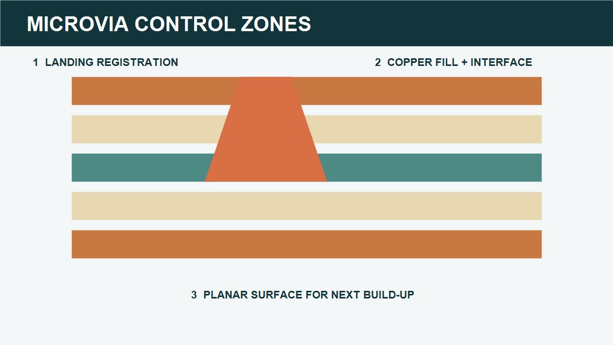
The hardest controls are cumulative. A small registration shift, incomplete cleaning or weak via fill can survive one stage and become inaccessible after the next lamination.
- Layer-to-layer registration: depends on artwork scaling, tooling, material movement and lamination history.
- Microvia landing: requires the drilled opening to meet the intended target pad after all movement is considered.
- Copper fill: must avoid voids and produce a surface compatible with the next layer or component pad.
- Planarity: matters for stacked structures and via-in-pad assembly surfaces.
- Fine-line control: requires imaging and etch compensation matched to copper thickness.
A supplier should explain its control plan for your construction, not answer only with a minimum-feature table. The DFM review process should close ambiguous via definitions before tooling.
How Does HDI Design Affect Reliability?
Reliability is shaped before production by via architecture, pad geometry, material pairing, copper balance and the number of thermal interfaces. The manufacturer can control a capable process, but cannot manufacture around an internally contradictory construction.
Stacked microvias concentrate interfaces vertically, while staggered structures trade board area for a different stress path. Via-in-pad can improve escape routing but makes fill and planarization part of the assembly surface requirement. Tight impedance targets also connect finished copper and dielectric variation to electrical performance; review the impedance-control checkpoints before release.
Which HDI Defects Should Engineers Watch For?
| Defect or signal | Likely process cause | How to verify | Buyer action |
|---|---|---|---|
| Microvia interface separation | Weak interface, contamination or thermal stress | Microsection and agreed reliability testing | Define coupon and acceptance plan |
| Void in filled via | Unstable plating/fill conditions | Cross-section or applicable X-ray evidence | Ask how fill integrity is sampled |
| Missed or marginal landing | Registration shift or inadequate target geometry | Sectioning and registration data | Review pad stack and scaling plan |
| Recessed or proud via fill | Fill and planarization variation | Surface/profile inspection | Define via-in-pad surface expectation |
| Impedance deviation | Dielectric or finished-copper variation | Coupon measurement and stack-up record | Approve production impedance structure |
The most useful defect report connects the observation to the released construction and corrective action. A generic “passed inspection” statement is weaker than traceable coupon, electrical-test and section evidence.
What Tests Verify HDI PCB Quality?
No single test proves an HDI build. Electrical test finds opens and shorts, while structural evidence checks whether the microvia and build-up were made as approved.
| Verification | What it checks | When to request it |
|---|---|---|
| AOI | Inner/outer pattern defects before burial or finish | Standard production control |
| Electrical test | Continuity and isolation | Every released netlist build |
| Microsection/coupon | Via geometry, interfaces and copper condition | New or critical HDI constructions |
| Impedance coupon test | Finished transmission-line result | Controlled-impedance designs |
| Thermal/reliability evaluation | Build response to the agreed stress profile | Qualification or high-reliability projects |
Acceptance must reference the drawing, purchase specification and agreed IPC class or project-specific requirement. For a broader test-method overview, see the PCB testing guide.
How Long Does HDI PCB Manufacturing Take?
HDI lead time is driven less by the word “prototype” than by engineering release, material availability, the number of sequential cycles, via-fill and planarization steps, coupon requirements and test holds.
- A 1+N+1 build generally has fewer repeated operations than 2+N+2 or a stacked any-layer construction.
- Material substitutions or an unresolved stack-up pause CAM and impedance work.
- New coupons, microsections or qualification tests add controlled waiting points.
- A quick quote is not the same as an approved production schedule.
Request a stage-based schedule after the stack-up and test plan are accepted. Do not compare suppliers using an advertised turnaround without confirming whether it includes engineering questions, special material procurement and qualification evidence.
What Files and Evidence Belong in an HDI RFQ?
A useful HDI RFQ lets the manufacturer quote the intended construction instead of guessing from Gerber layers.
- Gerber or ODB++ data and NC drill files
- Fabrication drawing with via start/stop layers and finished dimensions
- Proposed stack-up, materials, finished thickness and copper requirements
- Controlled-impedance table and reference layers
- Microvia type: staggered, stacked, via-in-pad, filled and capped as applicable
- Quantity, panel or delivery form and revision identity
- Surface finish, solder mask and marking requirements
- Inspection, coupon, microsection, electrical-test and reliability expectations
Use a consistent release package and revision table. This Gerber manufacturing guide explains the base handoff; HDI projects add explicit interconnect and stack-up definitions.
How Do You Evaluate an HDI PCB Manufacturer?
Evaluate whether the supplier can review, build and verify your construction—not whether its website lists HDI.
- Ask for a returned production stack-up and DFM questions before release.
- Confirm which via architectures and build-up cycles fit the actual design.
- Ask how microvia landing, fill integrity and planarity are sampled.
- Define the electrical, impedance, coupon and microsection evidence included.
- Confirm material and process changes require approval.
- Separate bare-board acceptance from optional assembly and functional testing.
PCBTRY’s HDI PCB manufacturing service is a relevant comparison-quote path when your package includes the stack-up, via structure and verification needs.
Frequently Asked Questions About HDI PCB Manufacturing
What makes HDI manufacturing different from standard multilayer PCB fabrication?
HDI repeatedly adds thin dielectric and copper layers, then forms microvias between selected layers. The repeated lamination, laser drilling, filling and registration controls create more interfaces than a conventional through-hole build.
Are all microvias laser drilled?
Laser drilling is the common method for small blind microvias in build-up dielectrics, but the approved method depends on material, geometry and supplier process. The drawing should define the connection rather than assume a machine choice.
Is a stacked microvia always better than a staggered microvia?
No. Stacked vias save routing area but add vertical interfaces and stricter fill/planarity demands. Staggered structures use more area and may simplify the vertical stack; choose from routing and reliability needs.
What causes microvia failures?
Possible causes include contamination, incomplete target preparation, weak metallization, fill voids, marginal landing and thermal stress. Root cause should be verified with sections, coupons and process history rather than inferred from electrical failure alone.
Does via-in-pad require filled and capped vias?
For a component pad to remain solderable and planar, the fabrication note commonly needs a defined fill and surface treatment. Confirm the exact structure with the fabricator and assembler before release.
How many sequential lamination cycles does an HDI board need?
The answer follows the build-up architecture, not total layer count alone. A 1+N+1 construction needs fewer repeated build-up operations than 2+N+2; the supplier should return the proposed cycle plan.
What evidence should accompany an HDI prototype?
At minimum, request the released stack-up, electrical-test status and agreed inspection records. Critical builds may also require impedance results, coupon sections, material identity and project-specific reliability evidence.
Can the same HDI stack-up move directly from prototype to volume?
It can when materials, process assumptions, panelization and acceptance evidence remain controlled. Before volume, review prototype deviations, yield risks and any proposed material or process changes.
Request an HDI Stack-Up and DFM Review
Send your Gerber or ODB++ data, drill files, fabrication drawing, proposed stack-up, impedance table, microvia definitions, quantity and test requirements to [email protected]. Ask for a returned production stack-up, DFM questions and a quotation that identifies the planned build-up cycles and verification evidence.



0 Comments