
Blog
Outer Layer PCB Process: Imaging, Copper Plating and Etch Checks
Follow the outer layer PCB process from dry-film imaging and copper pattern plating through tin stripping, etching, AOI and RFQ checks.



Follow the outer layer PCB process from dry-film imaging and copper pattern plating through tin stripping, etching, AOI and RFQ checks.
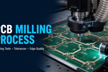
Learn how PCB milling controls routing data, cutter selection, compensation, feeds, tool wear, edge tolerances, burrs and finished-board inspection.
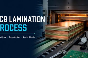
Learn how multilayer PCB lamination controls prepreg, resin flow, vacuum, temperature, pressure, registration, thickness, voids and delamination.
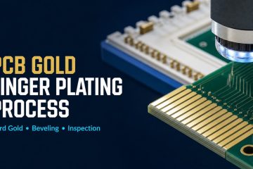
Learn how PCB gold fingers are selectively hard-gold plated over nickel, then beveled and inspected for thickness, adhesion, wear and connector fit.
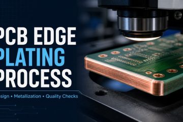
Learn how PCB edge plating is designed and manufactured, including wrap copper, profile preparation, metallization, finishes, defects and inspection.
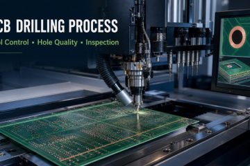
See how PCB drilling uses mechanical and laser processes, with controls for registration, tool wear, smear, hole quality, plating and inspection.
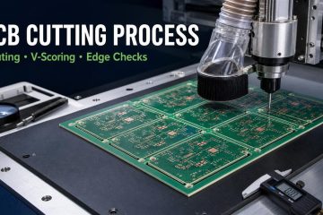
Learn how PCB cutting uses routing, V-scoring, laser and other methods, with controls for board stress, dimensions, edge quality and supplier approval.
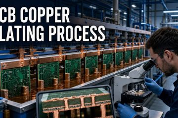
See how PCB copper plating builds conductive hole walls and circuits, including desmear, electroless copper, electroplating, bath control, defects and inspection.
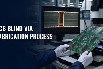
See how PCB blind vias are planned, drilled, desmeared, plated and tested—and what stack-up, DFM and supplier evidence to verify before production.
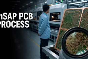
See how the mSAP PCB process builds fine copper features, where plating and flash etching fail, and what DFM files and inspection evidence to request.
If you have any enquiry about quotation or cooperation, please feel free to email us at [email protected] or use the following enquiry form. Oursales representative will contact you within 24 hours. Thank you for your interest in our products.