




The mSAP PCB process is a fine-line circuit-formation method that starts with a very thin conductive copper layer, builds copper only where traces are required, and then removes the exposed seed copper with a controlled flash etch. It is used when a dense HDI or substrate-like layout needs straighter trace sidewalls and smaller line/space than a conventional subtractive process can hold reliably.
The important question is not simply whether a factory “has mSAP.” Engineers need to know which layers require it, how the fabricator controls imaging, plating and flash etching, and what inspection evidence proves the finished geometry. Send your Gerber or ODB++ data, stack-up, impedance table, finished copper requirements and acceptance notes to [email protected] for a DFM feasibility review and quotation.
What Is the mSAP PCB Process?
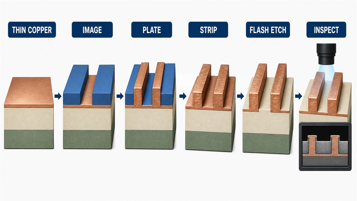
mSAP means modified semi-additive process. Instead of defining a trace by etching downward through relatively thick copper, mSAP begins with thin copper, patterns a resist mold, electroplates the trace upward, strips the resist, and removes only the thin copper left between traces.
This changes the geometry problem. Long subtractive etching attacks copper vertically and laterally, so a fine trace can become narrower at the top and wider at the base. mSAP limits the amount of copper that must be removed after pattern plating. The trace profile can therefore follow the imaged resist opening more closely. That benefit depends on the complete process window; the name mSAP alone does not guarantee a particular line width.
How Does the mSAP PCB Process Work?
The mSAP PCB process is a controlled sequence from layer mapping and thin-copper preparation through imaging, selective copper build-up, flash etching and inspection. Each stage changes the margin available to the next one.
1. Engineering review and layer mapping. CAM engineers identify the layers that actually need mSAP, review line/space, pad geometry, microvia targets, finished copper and impedance constraints, and select test coupons. Applying the process to every layer without need can add cost and risk. An incomplete layer map can also cause the fabricator to use the wrong compensation or copper construction.
2. Build-up dielectric and thin-copper preparation. The process needs a continuous conductive base with suitable adhesion to the dielectric. Surface condition, copper uniformity and carrier removal affect later plating and fine-line stability. Creases, particles or weak bonding can become opens, pits or lifted conductors after thermal processing. Material certificates and incoming inspection records are more useful than a generic claim of “ultra-thin copper.”
3. Microvia formation and metallization, when required. In an HDI build-up layer, laser drilling, desmear and electroless copper preparation occur before pattern plating. Residue at the via bottom can create weak or intermittent interconnection, while nonuniform seed coverage changes current distribution. A microsection through representative microvias helps verify target-pad condition and copper continuity.
4. Photoresist application and digital imaging. A uniform resist layer becomes the mold for the traces. Imaging must register the pattern to the actual panel and account for material movement. Dust, poor adhesion, incorrect exposure or weak development can distort an opening before copper is plated. The useful production evidence is registration data and AOI results, not the model name of the imaging machine.
5. Development and pre-plate inspection. Development removes resist from the areas where copper will be built. Residue narrows the plating channel; over-development can weaken the resist wall. Both defects alter finished line width. Pre-plate inspection should confirm clean openings, intact resist walls and alignment before the expensive copper build-up step.
6. Selective copper electroplating. Copper grows inside the resist openings to the specified conductor height, and microvias may be filled during the same broad plating stage depending on the construction. Current density, solution chemistry, agitation and panel loading influence thickness distribution and trace profile. Overplating can create mushroomed trace tops or close spacing; underplating reduces cross-sectional area and current margin.
7. Resist stripping and flash etching. After the resist is removed, a short controlled etch clears the thin exposed copper between traces. Too little removal leaves conductive remnants that can cause leakage or shorts. Too much removal reduces trace width or attacks the plated surface; nonuniform attack can create pits. A clean-looking panel is not enough—AOI, line-width measurement and cross-sections must confirm the result.
8. Inspection, lamination and downstream verification. The fine-line layer is inspected before it becomes inaccessible inside a multilayer stack. AOI checks opens, shorts and pattern deviations; dimensional measurement and cross-sections check copper geometry; electrical test verifies net continuity and isolation after the board is completed. The buyer should agree on coupon location, sampling and acceptance criteria before production.
| Process point | Main control | Failure signal | Evidence to request |
|---|---|---|---|
| Thin-copper base | Uniformity and adhesion | Lifted trace, crease, local open | Material construction and incoming inspection |
| Imaging/development | Registration and clean resist openings | Width shift, bridging, incomplete pattern | Registration report and pre-plate AOI |
| Pattern plating | Thickness distribution and trace profile | Low cross-section or mushrooming | Copper measurement and cross-section |
| Flash etch | Complete seed removal with limited trace attack | Residual copper, necking or pitting | AOI, width data and etched-surface micrograph |
How Is mSAP Different from SAP and Subtractive Etching?
The three methods differ mainly in the starting conductive layer and how much copper is removed to define the circuit. Select the process from the required feature geometry and production evidence, not from a fashionable process label.
| Method | How traces are formed | Best fit | Key trade-off |
|---|---|---|---|
| Subtractive | Image thick copper and etch unwanted copper away | Standard geometry and cost-sensitive layers | Lateral etch becomes harder to control as features shrink |
| mSAP | Plate traces on thin foil/seed, then flash-etch exposed base copper | Fine-line HDI and selected dense routing layers | More demanding materials, plating, cleanliness and inspection |
| SAP | Create a very thin seed on dielectric, plate the pattern and remove the seed | Still finer substrate-class structures | Higher process and material requirements; not automatically needed for a PCB |
If conventional routing already meets a qualified supplier’s production rules with margin, mSAP may not improve the project. A hybrid stack-up—mSAP only on the dense layers—often deserves evaluation.
Which Materials and Copper Structures Work with mSAP?
mSAP depends on a compatible thin-copper/dielectric system, stable build-up material and reliable copper adhesion. Material choice affects dimensional movement, laser drilling behavior, plating preparation, impedance and thermal reliability.
Do not substitute a generic laminate family late in the project. Ask the fabricator to identify the exact construction proposed for the fine-line layers, whether a carrier-backed foil or another seed structure is used, and how the material has been qualified with the planned via and surface treatment. For context on the base material, see this guide to copper-clad laminate structure.
How Should an mSAP Stack-Up Be Planned?
An mSAP stack-up should mark the fine-line layers, dielectric thicknesses, microvia sequence, copper targets and impedance references as one coordinated construction. Routing density alone is not a complete stack-up requirement.
Start by identifying the BGA escape or high-density routing layer that creates the constraint. Then verify reference-plane continuity, dielectric availability, via capture pads, sequential-lamination count and finished copper. Impedance modeling must use the fabricator’s proposed trace cross-section rather than assuming the trapezoid from a conventional process. If the design is HDI, review the broader HDI PCB design decisions before freezing the layer count.
What Fine-Line Design Details Need DFM Review?
DFM must review the complete geometry distribution, not only the single smallest trace. A minimum feature that appears thousands of times is a different yield risk from one isolated neck-down.
- Line/space by layer, including local neck-downs and copper density changes.
- Pad, via and capture-pad geometry around fine-pitch packages.
- Finished copper requirement, not only starting foil.
- Impedance targets, reference layers and allowed tolerance.
- Panel orientation, coupon requirements and critical net locations.
- Whether the same net can use wider conductors outside the dense escape region.
Provide Gerber or ODB++, drill data, stack-up, impedance table, fabrication drawing and acceptance notes together. A DRC pass in CAD is not proof of a supplier’s process capability; a formal PCB DFM review connects the design to the proposed manufacturing route.
What Are the Main mSAP Manufacturing Challenges?
The main challenges are contamination control, panel registration, resist integrity, plating uniformity, seed-layer removal and adhesion. They interact: an imaging defect can become a plating defect, and excessive flash etching can turn a small plating irregularity into a serious conductor loss.
- Particles and residues: can block a resist opening or interrupt the conductive path.
- Panel distortion: can shift fine features relative to vias and pads.
- Resist-wall failure: can widen or bridge plated conductors.
- Uneven current distribution: can create thin traces in one region and excessive build in another.
- Incomplete seed removal: can reduce electrical isolation between close conductors.
- Over-etch and pitting: can reduce cross-section and create stress concentration.
For a related explanation of lateral etch and CAM compensation, review PCB etch factor.
How Do Plating and Flash Etching Affect Reliability?
Plating creates the conductor that carries current; flash etching then removes the conductive base between traces. Reliability depends on keeping enough sound copper after both operations.
Nonuniform plating can reduce a trace below the intended cross-section even when its top-view width appears acceptable. Excessive or nonuniform flash etching can cause necking, pinholes or pits. These defects may increase resistance, change impedance, concentrate mechanical stress or weaken later stacking and surface treatment. That is why top-view AOI should be paired with thickness data and representative cross-sections for critical designs.
What Inspection and Test Evidence Should Buyers Request?
Request evidence that verifies geometry, copper integrity and electrical isolation at the appropriate stage. A final electrical test alone cannot show whether a trace has marginal cross-section.
| Evidence | What it confirms | What it cannot prove alone |
|---|---|---|
| AOI record | Pattern opens, shorts and dimensional deviations | Internal copper thickness or adhesion |
| Line-width/spacing data | Measured fine-feature distribution | Trace height and subsurface defects |
| Cross-section | Trace profile, copper build and microvia condition | Every location on every panel |
| Electrical test | Net continuity and isolation | Long-term margin of a thinned conductor |
| Impedance coupon | Transmission-line result for the agreed coupon | Unrepresented routing geometries |
Define sampling, coupon placement and pass/fail criteria in the purchase documentation. “AOI inspected” without a revision, result or acceptance rule is not a complete quality record.
How Long Does mSAP PCB Manufacturing Take?
There is no universal mSAP lead time. It depends on material availability, sequential build-up cycles, the number of mSAP layers, coupon and microsection requirements, engineering questions, prototype quantity and whether the supplier already has a qualified process for the proposed construction.
For a useful quotation, ask the supplier to separate engineering review, material procurement, fabrication and qualification-test time. A fast date given before stack-up and process review is less reliable than a schedule tied to approved data.
How Do You Qualify an mSAP PCB Manufacturer?
Qualify the supplier against your construction and evidence needs, not a headline minimum line/space. Ask these questions before release:
- Which exact layers and materials in this stack-up will use mSAP?
- What production rule—not a laboratory record—applies to the repeated fine geometry?
- How are panel movement and image registration measured and compensated?
- How are plating distribution and flash-etch completion monitored?
- Which cross-sections, coupons and AOI data will accompany prototypes or first articles?
- What change-control step applies if material or process chemistry must change?
- Which requirements should be relaxed to improve yield without changing function?
A capable engineering team should be able to return a marked-up stack-up or DFM note, explain the risk location, and propose measurable acceptance evidence.
mSAP PCB Process FAQ
Is mSAP the same as additive PCB manufacturing?
No. mSAP is a semi-additive family: copper is selectively built on a thin conductive base, and the exposed base copper is removed afterward. Fully additive approaches use a different starting and deposition route.
Does every HDI PCB need mSAP?
No. Many HDI boards can be produced with qualified subtractive or other fine-line processes. Use mSAP when the actual layer geometry, density and trace profile justify it.
Can mSAP improve controlled impedance?
Its more vertical and repeatable trace profile can make geometry easier to model, but impedance still depends on dielectric thickness, Dk, copper dimensions and process variation. Require a fabricator model and coupon plan.
What causes an mSAP open circuit?
Possible causes include contamination, incomplete resist development, weak seed continuity, local underplating, excessive flash etching or handling damage. Failure analysis should locate the defect and inspect its cross-section rather than guess from the electrical symptom.
What causes shorts between mSAP traces?
Residual seed copper, resist bridging defects, plating overgrowth or imaging errors can reduce isolation. AOI and electrical isolation testing detect different parts of this risk.
What files are needed for an mSAP quote?
Send Gerber or ODB++, drill files, stack-up, finished copper, impedance requirements, fabrication drawing, quantity, material constraints and acceptance/test notes. Highlight the layers and regions that require the smallest geometry.
Should a buyer specify an exact mSAP recipe?
Usually specify the functional geometry, materials, copper, reliability and acceptance evidence, then let the qualified fabricator propose the process. Recipe-level control is appropriate only when your validated product specification requires it.
Can mSAP be used on only selected PCB layers?
Yes, and selective use may reduce cost and process exposure. The stack-up and sequential-lamination plan must still be reviewed as a complete system.
Send the Right Data for an mSAP DFM Review
For an engineering assessment, send Gerber or ODB++, NC drill data, the proposed stack-up, impedance table, finished copper requirements, material constraints, quantities and acceptance notes. Mark the critical fine-line layers and BGA escape regions. Email [email protected] and request an mSAP feasibility review, evidence plan and quotation before freezing the board release.



0 Comments