




The PCB copper plating process converts drilled, nonconductive hole walls into reliable vertical interconnections and builds copper on selected circuit features. It combines surface preparation, metallization and electrolytic deposition; the result depends as much on drilling, desmear and current distribution as on the copper bath itself.
For multilayer, HDI, high-current and high-reliability boards, plating quality affects via life, current capacity, thermal cycling and final yield. PCBtry can review Gerber or ODB++, drill files, stackup, finished copper requirements and inspection notes before quotation so the plating route and evidence plan match the design.
What Is the PCB Copper Plating Process?
PCB copper plating is the controlled deposition of copper onto conductive surfaces and previously nonconductive drilled hole walls. A thin chemical or direct-metallization layer first makes the hole wall conductive; electrolytic plating then builds copper to the required product specification.
It should not be confused with laminate copper foil, final surface finish or solder filling. The starting foil is part of the laminate, copper plating adds metal during fabrication, and finishes such as ENIG protect exposed pads later.
How Does the PCB Copper Plating Process Work?
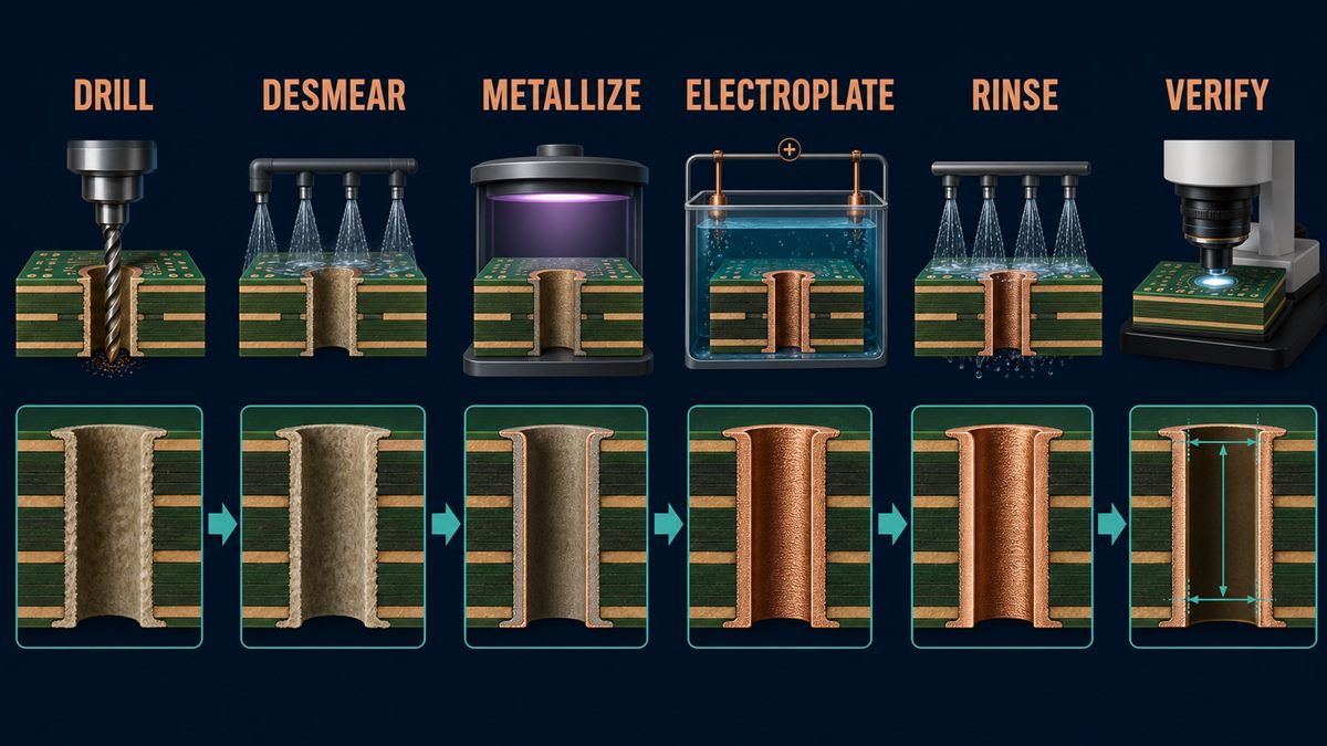
The process works as one connected sequence. A defect created during drilling or cleaning can remain hidden until microsection, thermal stress or field use, so each stage must be released before the next.
1. Engineering review and plating-route selection. CAM engineers review hole sizes, aspect ratios, layer count, copper weights, via types, impedance features and finished thickness requirements. They decide whether panel plating, pattern plating, via filling or another qualified route is appropriate. If the drawing mixes base copper with finished copper, the supplier may build the wrong etch/plating allowance.
2. Drilling and hole-wall condition. Mechanical or laser drilling creates the interconnect geometry. Smear, glass-fiber protrusion, roughness, debris and damaged inner-layer copper can prevent continuous metallization. Plating cannot reliably repair a torn or contaminated hole wall.
3. Desmear and conditioning. The hole walls are cleaned and resin smear is removed so inner-layer copper is exposed and the dielectric surface can accept activation. Excessive treatment can attack resin or glass interfaces; insufficient treatment can leave weak or missing connections.
4. Activation and initial metallization. A catalytic or direct-metallization process creates a conductive path on the dielectric. In an electroless route, chemical copper deposits without external current. Coverage must be continuous through the hole; voids at this stage can remain after later build-up.
5. Electrolytic copper build. Panels become cathodes in the copper-plating cell. Current drives copper ions onto the conductive surfaces and hole walls. Bath chemistry, agitation, temperature, current density, anode condition, panel loading and contact quality affect deposit structure and uniformity.
6. Panel or pattern plating control. Panel plating adds copper broadly before imaging/etching; pattern plating builds copper on exposed circuit features after imaging. The route changes etch allowance, trace geometry and process sequence. Buyers should evaluate the finished structure rather than assume one route is universally superior.
7. Rinse, protection and downstream transfer. Rinsing prevents drag-in and chemical carryover. Pattern-plated copper may receive an etch-resist metal before resist stripping and etching. Poor rinsing or delayed transfer can stain, oxidize or contaminate the surface.
8. Inspection and release. Thickness measurements, microsections, visual inspection, electrical test and any specified reliability testing confirm the deposit. A continuity pass alone cannot prove adequate copper thickness or freedom from hidden voids.
| Process stage | Main control | Failure risk | Buyer evidence |
|---|---|---|---|
| Drill/desmear | Clean, exposed hole wall and inner-layer interface | Smear, roughness, weak interconnect | Qualified drill/desmear route and microsection |
| Initial metallization | Continuous conductive coverage | Void or skip plating | Process monitoring and section evidence |
| Electroplating | Bath, current, agitation and loading | Thin center, nodules, burning, poor ductility | Bath/control records and thickness data |
| Rinse/transfer | Low carryover and protected surface | Stain, contamination, adhesion loss | Line control and visual criteria |
| Release | Requirement-specific sampling/testing | Hidden weak barrel despite continuity | Microsection, electrical and specified reliability results |
What Is the Difference Between Electroless and Electrolytic Copper?
Electroless copper creates conductive coverage through a chemical reaction without external current; electrolytic copper uses electrical current to build a thicker deposit on an already conductive surface. They are complementary stages in many PCB routes, not competing names for the same operation.
| Factor | Electroless/direct metallization stage | Electrolytic copper stage |
|---|---|---|
| Primary job | Make dielectric hole walls conductive | Build copper to the specified structure |
| Key risk | Incomplete activation or coverage | Nonuniform thickness, roughness or poor deposit properties |
| Geometry concern | Access and coverage through the hole | Current distribution and throwing power |
| Evidence | Continuity of initial coverage/process control | Thickness, microstructure and finished-hole evidence |
How Do Panel Plating and Pattern Plating Affect the Board?
Panel plating deposits copper across the panel before the final circuit pattern is etched, while pattern plating deposits additional copper only on imaged, exposed features. The chosen route affects copper distribution, trace etching, resist requirements and manufacturability.
Fine lines, heavy copper, high layer counts and special via structures may favor different process choices. The decision belongs in CAM/DFM review. If trace width, finished copper or impedance depends on the route, record it explicitly rather than approving only a generic copper weight.
What Controls Copper Thickness and Uniformity?
Uniformity depends on hole geometry, electrical contact, panel layout, current distribution, bath condition, agitation and plating time. High-aspect-ratio holes are harder to plate uniformly because solution exchange and current distribution inside the barrel differ from the outer surface.
Thieving, shielding, panel orientation and optimized racks can improve distribution, but they do not remove the need for design limits. For related design decisions, review how to choose PCB copper thickness and how via geometry and plating affect DFM.
What Copper Plating Defects Cause Reliability Failures?
The most important defects are voids, thin barrel regions, poor inner-layer connection, cracks, rough/nodular deposits, burned areas and adhesion loss. Their visible symptom may appear only after assembly reflow or thermal cycling.
| Defect | Possible origin | Consequence | Useful check |
|---|---|---|---|
| Void/skip plating | Contamination, trapped gas, incomplete activation | Intermittent/open via | Microsection and electrical test |
| Thin barrel center | High aspect ratio or weak throwing power | Thermal-cycle crack risk | Minimum-point thickness measurement |
| Weak inner-layer interface | Residual smear or damaged copper | Connection separation | Interface-focused microsection |
| Nodule/rough copper | Bath particles or current/process imbalance | Local stress, reduced clearance | Visual/section inspection and bath control |
| Overplating | Excess build or distribution imbalance | Finished-hole/trace geometry change | Finished dimension and copper measurement |
How Does Design Affect Plating Reliability?
Design sets the plating difficulty before production starts. Small holes through thick boards, mixed hole sizes, dense copper distribution, blind/buried structures and very heavy finished copper can narrow the process window.
Provide finished-hole size rather than only drill size, identify press-fit or controlled-impedance features, state whether copper values are base or finished, and include coupons/acceptance notes when required. Do not copy a generic aspect-ratio limit from another supplier; confirm the actual stackup and qualified capability.
How Is PCB Copper Plating Inspected?
Inspection combines process evidence with finished-product evidence. XRF or other approved measurement can assess accessible surface deposits; microsection exposes barrel thickness, interfaces, voids and internal geometry; electrical test checks connectivity. Each method answers a different question.
Request the sample location, measurement points, applicable test method, acceptance class and actual result. A polished section should be prepared without smearing or rounding that distorts the deposit. For high-current builds, complement section evidence with the appropriate electrical/thermal checks described in the heavy-copper testing process.
How Do You Choose a Copper Plating Supplier?
Choose a supplier that can link design geometry to a qualified plating route and return objective evidence, not one that answers only with a maximum copper number.
- Ask which hole sizes, aspect ratios and via structures are qualified on the proposed stackup.
- Confirm how drill/desmear, activation, bath chemistry, current, racks and rinse quality are controlled.
- Define base copper versus finished copper and the measurement location.
- Request microsection coupons and sampling appropriate to the product class.
- Ask how nonuniform panels, edge effects and mixed features are compensated.
- Confirm change control for chemistry, equipment, material and process-route changes.
- Review defect containment, lot traceability and requalification evidence.
How Long Does Copper Plating Take?
Plating time cannot be quoted responsibly from the keyword alone. Prototype and production lead time depends on the complete stackup, hole geometry, copper build, panel loading, via filling, coupons, inspection and any reliability testing. Heavy build or complex blind/buried structures may add cycles and verification.
Submit complete fabrication data so the supplier can separate normal line time from engineering review, special plating, microsection and approval time.
PCB Copper Plating Process FAQ
Why are PCB holes plated with copper?
Copper connects pads and internal layers through the board and provides a solderable conductive barrel where required. The drilled dielectric wall must first be metallized because it is not conductive.
Is electroless copper the final hole-wall copper?
Usually it is the initial conductive layer for a later electrolytic build. The exact route depends on the manufacturer’s qualified process.
What causes plating voids?
Contamination, smear, incomplete activation, trapped gas, poor solution access and process instability can contribute. Root cause must be traced to the actual stage and evidence.
Can electrical test prove plating thickness?
No. It can confirm connectivity at test time but cannot show minimum barrel thickness or hidden interface quality. Microsection or another specified method is needed for structure.
Does more copper always improve reliability?
No. The deposit must meet geometry and material requirements with suitable uniformity and properties. Excess or nonuniform plating can affect holes, traces and later processing.
What files are needed for a plating quotation?
Send Gerber or ODB++, NC drill/rout files, stackup, finished thickness, base/finished copper definitions, hole tolerances, via requirements, quantities and inspection/class notes.
How are high-aspect-ratio holes checked?
Suppliers should evaluate the proposed geometry against a qualified process and verify minimum barrel regions with appropriate coupons and microsections.
What should a microsection report identify?
It should identify the lot/coupon, sample location, magnification or method, relevant interfaces, measured copper and the acceptance requirement used.
Send Your PCB Data for a Plating Review
Send Gerber or ODB++, drill files, stackup, finished-hole tolerances, copper definitions, via structures, quantities and inspection requirements to [email protected]. Request a copper-plating DFM review, evidence plan and quotation before releasing production.



0 Comments