




The PCB drilling process creates vias, component holes, tooling holes, mounting holes, slots, and—in advanced constructions—blind or microvia features that connect selected layers. Mechanical drills remove copper, resin, and reinforcement with a rotating tool; lasers ablate material for qualified small or controlled-depth features. Hole quality matters because drilling is the foundation for desmear, copper deposition, plating, component fit, and interlayer reliability.
PCBtry reviews NC drill data, stackup, finished-hole requirements, aspect ratio, via type, material, registration, plating, and inspection notes before releasing a drill program. Send Gerber or ODB++ data, drill files, fabrication drawing, stackup, quantities, and acceptance requirements for a DFM review and quotation.
What Features Does PCB Drilling Create?
Drilling creates plated and non-plated features with different functions and controls. A via connects copper layers; a component hole must fit a lead after plating; a mounting or tooling hole may remain unplated; a slot has length, width, end geometry, and plating status. The fabrication drawing must distinguish finished size from production drill size because plated holes receive copper after drilling.
When Should Mechanical or Laser Drilling Be Used?
Mechanical drilling fits many through holes and mechanical features, while laser drilling is considered for qualified microvias and controlled-depth HDI structures. The decision depends on finished geometry, depth, material response, pad design, stackup, reliability, and supplier capability.
| Route | Typical fit | Main control | Main risk |
|---|---|---|---|
| Mechanical drilling | Through vias, component, tooling, mounting holes and slots | Tool geometry/life, spindle, feed, entry/backup, registration | Wear, breakage, burr, smear, wander and rough walls |
| Laser drilling | Qualified blind microvias and dense HDI structures | Energy, focus, pulse, target depth, material absorption and cleaning | Residue, carbonization, copper damage, inconsistent diameter/depth |
| Controlled-depth mechanical | Selected blind features where stackup and depth allow | Z-depth calibration, panel flatness and stop-layer protection | Depth variation or target-layer damage |
| Sequential drilling | Buried features drilled before later lamination | Build sequence and registration through each cycle | Stackup/revision error discovered after lamination |
How Does the PCB Drilling Process Work?
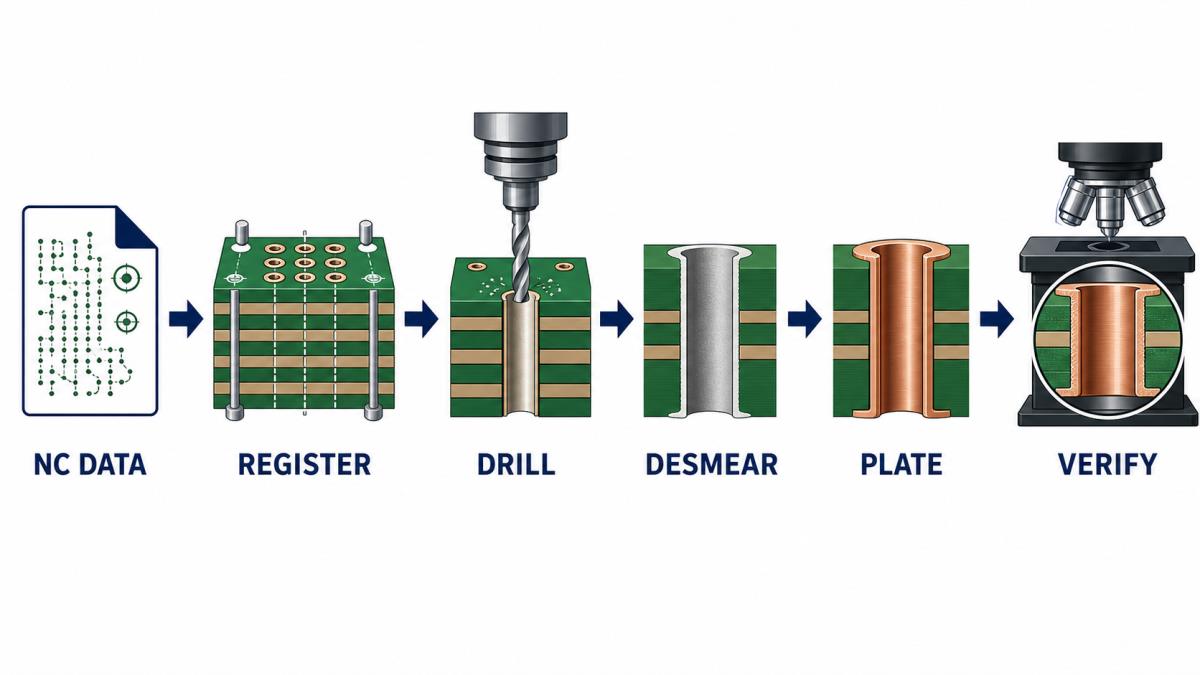
The process converts released design data into verified holes while protecting registration and hole-wall condition for later metallization.
Step 1: Validate drill data. CAM checks tool codes, plated/non-plated classification, duplicate or missing hits, slot definitions, finished sizes, outline relationship, and drawing conflicts.
Step 2: Plan the drill route. Engineering assigns mechanical, laser, controlled-depth, or sequential operations and chooses panel stack, entry/backup material, tooling, and inspection.
Step 3: Register and stack panels. Panels are aligned to the released datum; stack height and support must keep positional accuracy and chip evacuation stable.
Step 4: Prepare tools and programs. Drill diameter, geometry, tool-life rule, spindle/feed recipe, hit sequence, and change points are controlled by material and construction.
Step 5: Drill a first panel. Position, diameter, burr, wall condition, and target depth where relevant are checked before volume release.
Step 6: Drill with tool-life monitoring. Tools are changed by the qualified rule rather than after visible failure. Broken-tool and program alarms prevent unrecorded missing holes.
Step 7: Clean and desmear. Debris and resin smear are removed so inner-layer copper is exposed and the hole wall can accept metallization.
Step 8: Plate and verify. After electroless copper and electroplating, microsections, electrical test, and other specified checks verify the complete plated structure—not merely the drilled opening.
Why Are NC Drill Data and Registration Critical?
The NC drill file controls tool locations and sizes, while copper artwork and the drawing define what those hits must connect or avoid. An origin, format, unit, zero-suppression, revision, or plated-status mismatch can shift an otherwise accurate drill program. CAM should compare drill data against pads, clearances, slots, and the board outline before release.
For multilayers, registration also depends on inner-layer imaging, lamination movement, tooling, and drill alignment. The buyer should specify the functional tolerance or annular-ring requirement and let the fabricator confirm a manufacturable stack and compensation plan.
How Do Material and Stackup Affect Hole Quality?
Glass weave, resin system, copper thickness, total thickness, flex materials, metal layers, and ceramic constituents change cutting load, heat, wear, debris, and desmear response. A recipe qualified on standard FR-4 should not be assumed for high-Tg, high-frequency, polyimide, heavy-copper, or mixed-material constructions.
Stack height also affects chip removal, tool deflection, and positional consistency. The supplier should qualify entry/backup materials, panel count, tool life, and desmear to the actual construction rather than applying a universal number.
How Are Drill Tools and Machine Conditions Controlled?
Tool control links each drill bit to diameter, geometry, material route, allowed use, and change history. Wear can worsen location, wall roughness, burr, heat, smear, and nail heading before the bit breaks. A factory therefore uses a qualified life rule plus first-piece and in-process checks.
Spindle condition, runout, feed, rotational speed, retract behavior, panel support, vacuum/chip extraction, entry/backup condition, and temperature all affect the cut. Buyers do not need proprietary recipes, but they can request evidence that tools and machines are controlled by revision and lot.
Why Must Drilled Holes Be Desmeared Before Plating?
Desmear removes resin deposited over exposed inner-layer copper and conditions the dielectric wall for reliable metallization. If residue remains, deposited copper may not bond or connect correctly, causing plating voids, intermittent opens, or reduced thermal-cycle life.
The chemistry or plasma route must match the resin system and hole construction. Excess treatment can attack material or alter geometry; insufficient treatment leaves contamination. Cross-sections and process coupons help confirm the combined drill-desmear-plating result.
What Drilling Defects Threaten Reliability?
| Defect | Possible cause | Risk | Control/evidence |
|---|---|---|---|
| Smear | Drill heat/wear or inadequate desmear | Poor inner-layer connection | Qualified desmear and microsection |
| Nail heading | Mechanical deformation of inner-layer copper | Stress/conductor damage | Tool/recipe control and cross-section |
| Burr | Dull tool, poor support or entry/exit condition | Plating/lamination handling defects | Tool life and visual inspection |
| Breakout/misregistration | Data, lamination, tooling or drill-position error | Reduced or missing annular connection | CAM check, registration coupon, AOI/microsection |
| Rough wall/glass protrusion | Wear, recipe or material mismatch | Nonuniform plating and crack initiation | Qualified material route and cross-section |
| Missing/blocked hole | Broken tool, debris or program issue | Open circuit or assembly failure | Broken-tool detection and electrical/visual test |
How Is Hole Quality Inspected?
Inspection combines data verification, dimensional checks, visual or optical review, microsection, and electrical testing according to feature risk. Before plating, the factory can check position, diameter, burr, depth, and debris. After plating, a cross-section can show wall condition, inner-layer connection, copper coverage, voids, and structural damage.
Electrical test verifies network continuity and isolation but cannot describe every physical weakness. Specify the acceptance standard, coupon, sample plan, controlled dimensions, report, and any reliability testing in the RFQ.
How Does PCB Design Affect Drilling Yield?
Hole-to-thickness relationship, pad size, annular ring, hole-to-copper clearance, density, via type, stackup, and tolerance determine manufacturability. A finished hole that leaves too little room for production drill/plating variation can drive breakout or plating risk.
Use fabricator-approved pad and via rules, separate plated from non-plated data, avoid ambiguous slots, and review HDI structures early. PCBtry’s blind-via fabrication process and via manufacturing guide provide related design context.
What Should Buyers Ask a PCB Drilling Supplier?
Send the complete fabrication package and ask the supplier to identify the proposed drill route, data conflicts, finished-vs-production size interpretation, stackup constraints, tool-life control, desmear route, plating sequence, and inspection evidence.
- Gerber/ODB++, NC drill/rout data and fabrication drawing.
- Stackup, material, copper, finished thickness and quantities.
- Plated/non-plated classification, finished hole/slot sizes and tolerances.
- Blind, buried, microvia, filled/capped, backdrill and controlled-depth definitions.
- Impedance/coupon, cross-section, electrical test and report requirements.
Frequently Asked Questions
Is drill size the same as finished hole size?
Not necessarily. A plated hole is drilled larger before copper is deposited; the drawing should state the required finished size and tolerance. The fabricator selects the production drill using the plating route.
Why do PCB drill bits wear quickly?
They cut abrasive reinforcement, copper, and resin at small diameters and high cycles. Material, tool geometry, heat, chip evacuation, entry/backup and machine condition determine the qualified life.
What is drill smear?
Smear is resin transferred over the hole wall and exposed inner-layer copper during drilling. It must be removed before metallization so copper can form a reliable interlayer connection.
Can all microvias be laser drilled?
Laser drilling is common for qualified microvia constructions, but material, copper opening, depth, diameter, stackup, fill and reliability requirements must be reviewed together.
How are blind holes stopped at the correct depth?
The route may use sequential construction, laser targeting, or controlled-depth mechanical drilling. The selected method depends on the stackup and must protect the target copper layer.
What detects missing drilled holes?
Program verification, broken-tool monitoring, optical inspection and later electrical test work together. Each method detects a different failure mode.
Does electrical test prove hole-wall quality?
It proves network behavior at test conditions but may not reveal every marginal physical structure. Microsections, coupons and reliability tests provide complementary evidence when required.
What files are needed for drilling review?
Provide NC drill/rout data, Gerber or ODB++, fabrication drawing, stackup, material, finished sizes/tolerances, via definitions, quantities and test/inspection requirements.
Request a PCB Drilling DFM Review
Send PCBtry your fabrication package and ask for a drill-data, stackup, via-structure, desmear, plating, and inspection review. The quotation can then reflect the actual hole construction instead of a generic minimum-hole claim.



1 Comment
PCB Plated Through-Hole Process: Drilling, Copper Plating and Reliability Checks - thindry pcb manufacturer · 09/01/2026 at 15:45
[…] or repeated thermal-cycle applications early. For the upstream hole-formation context, review the PCB drilling process; for assembly implications, see the through-hole assembly […]