




The PCB gold finger plating process creates wear-resistant contact pads for a card-edge connector by selectively electroplating nickel and hard gold onto defined copper fingers. Unlike ENIG on solder pads, the contact finish must tolerate sliding, repeated mating and localized contact force. The result depends on the connector drawing, temporary plating access, deposit control, board profile and inspection—not on gold color alone.
PCBTRY combines fabrication-data review, panel planning, selective plating, profiling and bare-board inspection. Send the Gerber or ODB++ package, fabrication drawing, mating-connector specification, finish callout, bevel detail, quantity and acceptance requirements for a DFM review and quotation.
What Is the PCB Gold Finger Plating Process?
Gold finger plating is a selective electrolytic finish applied to exposed edge-connector contacts. A nickel underplate separates the gold from copper and supports the contact surface; the outer hard-gold alloy is selected for wear resistance. The exact deposit, geometry and acceptance limits must come from the product drawing or agreed specification.
This is not simply an alternative color for ENIG. Immersion gold is a solderable protective finish, while an edge connector that slides against spring contacts normally needs a wear-oriented contact system. The mating connector, expected cycles, environment and product class determine the requirement.
How Does the PCB Gold Finger Plating Process Work?
The process succeeds when design data, electrical plating access and mechanical profiling are planned together.
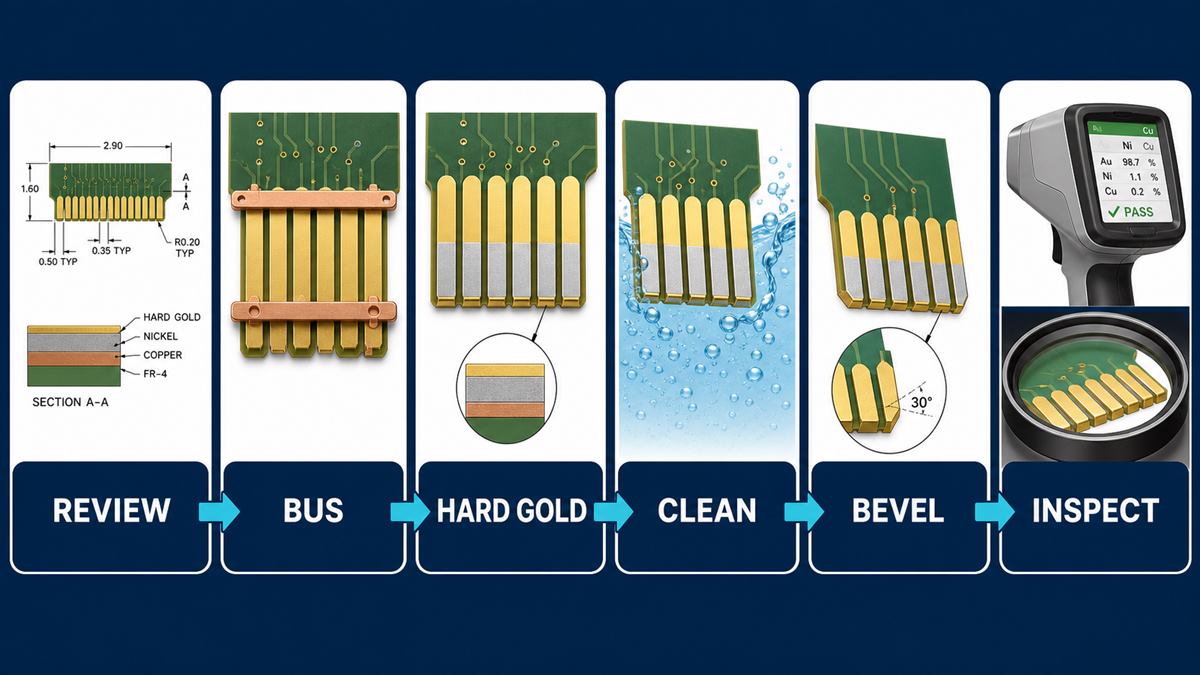
1. Engineering review and connector-data check. CAM compares finger pitch, contact length, board thickness, datum, edge location, bevel and finish notes with the connector drawing. An ambiguous “gold fingers” note is not enough: the shop needs to know which pads are contacts and what evidence is required. A mismatch here becomes poor engagement, incomplete wiping or an unquotable finish.
2. Panelization and plating-access design. Electrolytic plating requires every finger to be electrically connected to the plating circuit. The fabricator plans temporary tie bars, bussing or panel-edge connections that will later be removed. Segmented or recessed fingers may need special CAM treatment; inaccessible contacts can plate unevenly or require a different panel scheme.
3. Outer-layer imaging and copper preparation. The finger pattern is imaged and etched with the rest of the outer circuitry, then cleaned to expose sound copper. Residue, oxidation, damaged resist edges or excessive undercut changes deposit adhesion and contact geometry. The inspection point is the finished copper pattern, not only the artwork.
4. Selective masking. Areas that must not receive hard gold are protected while the contact zone remains exposed. Mask registration controls the finish boundary. Poor masking produces gold spread, exposed transition copper or an irregular line that can interfere with solder mask and assembly features.
5. Nickel underplating. Electrolytic nickel is deposited as the barrier and mechanical foundation. Bath condition, current distribution, surface activation and time determine uniformity. Thin, porous or poorly adhered nickel can permit copper migration or allow the contact finish to fail during wear.
6. Hard-gold electroplating. Hard gold is deposited to the drawing requirement while current density, solution chemistry, agitation and time are controlled. Edge effects and current crowding can make deposit thickness vary across a finger array. Excessive current may create a rough or burned surface; insufficient coverage can leave thin areas and pinholes.
7. Resist stripping, cleaning and the remaining surface finish. Temporary masks are removed without scratching the contacts. Solderable areas may receive ENIG, HASL, OSP or another finish through a controlled sequence that protects the hard-gold region. Cleaning must remove chemical residues without attacking the plated surface.
8. Profiling, beveling and final inspection. Routing removes temporary plating connections and creates the final edge. If the connector requires a bevel, the angle, depth and termination point follow its drawing. A dull or misaligned tool can chip the laminate, expose copper or scrape the finger. Final checks cover geometry, finish condition, thickness evidence, electrical continuity and cleanliness.
What Files and Callouts Does the Fabricator Need?
| Input | What it must define | Risk if missing |
|---|---|---|
| Gerber/ODB++ and drill/rout | Finger copper, mask openings, final outline and slots | Wrong contact geometry or inaccessible plating path |
| Fabrication drawing | Finish type, nickel/gold requirement, bevel and datum | Supplier assumptions replace product intent |
| Connector drawing | Board thickness, engagement depth, contact pattern and edge detail | Mechanical fit or wiping failure |
| Acceptance package | Class, visual limits, thickness report, coupon or other evidence | No objective release basis |
| Lifecycle/environment | Mating cycles, corrosion exposure and cleaning restrictions | Finish selected for the wrong duty |
Put controlled requirements on the fabrication drawing rather than relying on order-form comments. PCBTRY’s gold finger design guide can help organize connector geometry before release.
Why Are Hard Gold and ENIG Not Interchangeable?
Hard gold is electrodeposited for contact wear; ENIG uses an immersion-gold layer primarily to protect nickel and provide solderability. A connector contact rubs during insertion, so the finish must withstand mechanical wiping as well as corrosion. A drawing that says only “gold” leaves the supplier without the functional requirement.
The rest of the PCB can still use a solderable finish while only the fingers receive selective hard gold. That combination changes masking and process sequence, so identify both finishes and their boundaries.
How Do Panelization and Tie Bars Affect the Result?
Every electrolytically plated finger needs a current path. Temporary bussing is commonly placed outside the final outline, then removed during routing. The panel must also provide gripping, plating and bevel-tool access without exposing the finished contacts to handling damage.
Do not delete an apparently unwanted edge connection from CAM without asking why it exists. Ask the supplier to show where plating connections will be removed and whether their removal can leave copper witness marks in a controlled area.
What Defects Occur in Gold Finger Plating?
| Observed defect | Likely control area | Why it matters | Evidence to request |
|---|---|---|---|
| Thin or nonuniform gold | Current distribution, access or bath control | Uneven wear and corrosion protection | Thickness map/report and lot traceability |
| Pinholes or pores | Surface preparation or deposit quality | Underlying metal can corrode | Visual/porosity method if specified |
| Rough or burned surface | Excess current density or bath condition | Unstable contact and accelerated wear | Magnified inspection and process disposition |
| Peeling or blistering | Activation, contamination or nickel adhesion | Finish can detach during mating | Adhesion test or agreed coupon evidence |
| Scratched fingers | Handling, routing or beveling | Exposes the system to wear/corrosion | 100% visual inspection criteria |
| Chipped bevel or exposed copper | Tool, datum or profile sequence | Poor insertion and connector damage | Edge profile measurement and photos |
How Are Gold Fingers Inspected?
Inspection should combine complementary methods. Visual or AOI checks find scratches, contamination, pits, mask encroachment and geometry errors. X-ray fluorescence or another agreed method verifies deposit thickness without relying on appearance. Profile measurement confirms board thickness, finger location and bevel; electrical test confirms continuity and isolation.
High-reliability programs may add adhesion, porosity, contact-resistance, environmental or mating-cycle tests when the drawing requires them. Do not claim these tests are automatic: define the method, sample plan, acceptance limit and report in the purchase package.
How Does Beveling Affect Contact Reliability?
The bevel guides the PCB into spring contacts and reduces scraping at the leading edge. Its angle and termination depend on the connector—not a universal shop preference. Too deep a bevel can shorten the functional contact land; too shallow or rough an edge can increase insertion force and damage the plating.
Beveling also interacts with final routing and panel support. Review PCBTRY’s PCB cutting process for routing and edge-quality controls, and show the bevel datum directly on the fabrication drawing.
How Should Buyers Compare Gold Finger Suppliers?
- Can engineering review the connector drawing, plating access and bevel together?
- Can the supplier separate hard-gold contacts from the board’s solderable finish?
- How are current distribution, bath condition and thickness uniformity controlled?
- Which measurement method and sample plan support the thickness report?
- How are scratches, pinholes, exposed copper and bevel damage dispositioned?
- Can the supplier preserve lot, chemistry and inspection traceability?
- Will it return a marked-up DFM report before tooling when data conflict?
Related copper deposition fundamentals are covered in PCBTRY’s PCB copper plating process; selective hard gold adds contact-specific materials, masking and wear controls.
Gold Finger Plating FAQ
Are PCB gold fingers made with pure gold?
Wear contacts normally use an electrodeposited hard-gold system over nickel, but the exact alloy and deposit requirements must be specified. Do not infer composition from color.
Can ENIG be used instead of hard gold?
ENIG may suit some one-time or non-wiping applications, but repeated card-edge mating normally needs a wear-oriented finish. Confirm against the connector and lifecycle requirement.
Why does the fabricator need plating tie bars?
Electrolytic deposition requires a current path to each finger. Temporary connections outside the final profile provide that path and are removed later.
Should beveling occur before or after plating?
The supplier selects a qualified sequence that protects the finished contact and meets the drawing. The buyer should specify the final geometry and acceptance condition rather than dictate an unverified generic sequence.
What causes gold finger peeling?
Contamination, weak surface activation, poor nickel adhesion or mechanical damage can contribute. Failure analysis should identify the interface and compare it with process and adhesion evidence.
How is gold thickness measured?
XRF is commonly used for nondestructive deposit measurement, but the purchase package should define locations, sampling and reporting. Appearance alone cannot verify thickness.
What files are needed for a quotation?
Send fabrication data, drill/rout, fabrication drawing, connector drawing, stackup, finish/bevel notes, quantity and requested reports. Add lifecycle or environmental requirements when they drive the finish.
What most often delays a gold finger order?
Unclear “gold” callouts, missing bevel details, incompatible connector thickness, inaccessible plating geometry and undefined inspection requirements cause engineering holds.
Request a Gold Finger DFM and Quotation
Send your fabrication package, connector drawing, finish and bevel callouts, quantities and acceptance evidence to PCBTRY. Engineering can review contact geometry, plating access, process sequence and inspection requirements before the panel enters production.



0 Comments