




The PCB soldering process creates electrical and mechanical joints between component terminations and PCB pads. In production, that may mean solder-paste printing and reflow for SMT, wave or selective soldering for through-hole parts, and controlled hand soldering for prototypes or rework. The correct route depends on component mix, board thermal mass, bottom-side clearance, cleanliness requirements and inspection access—not simply production volume.
For an assembly review, send PCBTRY the Gerber or ODB++ data, BOM, centroid/CPL file, assembly drawings, approved solder alloy and flux requirements, component datasheets, panel information and test criteria. These inputs allow the engineering team to review paste apertures, thermal risks, through-hole access and inspection coverage before quotation.
What Is the PCB Soldering Process?
PCB soldering is a controlled joining process: flux prepares the metal surfaces, heat raises the solder above its working range, molten solder wets compatible finishes, and cooling forms the joint. A shiny appearance alone does not prove reliability. Pad design, surface finish, paste deposit, component termination, heat history and contamination all influence the result.
How Does the PCB Soldering Process Work?
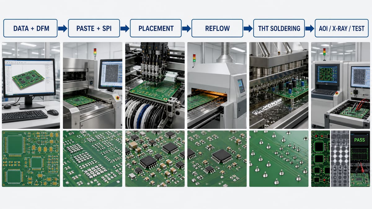
1. Data and DFM review. Engineering aligns the BOM, CPL, Gerber data, polarity information and assembly drawings. The review identifies mixed technologies, heat-sensitive parts, bottom-terminated packages and connectors that may block wave or selective-solder access. Unresolved package or polarity conflicts should stop release.
2. Material and process-route selection. The assembler confirms solder alloy, paste, flux and cleaning route, then decides which joints use reflow, wave, selective or hand soldering. Mixing materials without checking compatibility can change wetting, residue behavior and thermal limits.
3. Solder-paste printing and inspection. A stencil deposits paste on SMT pads. Aperture design, stencil condition, board support and print alignment control deposit volume. SPI can identify insufficient paste, excess paste and offset before components consume time and value downstream.
4. Component placement. Pick-and-place equipment positions parts in the paste. Package data, feeder setup, nozzle choice and placement coordinates matter. A part may appear centered but still have reversed polarity, incorrect rotation or marginal lead-to-pad overlap.
5. Reflow soldering. The assembly travels through a profiled oven so flux activates, solvents escape, solder melts and joints cool without overstressing components or laminate. The profile must reflect the actual board, component mix and solder system; a generic oven recipe can create non-wetting, voiding, tombstoning or component damage.
6. Through-hole soldering. Wave soldering treats many accessible joints together, while selective soldering targets defined areas around mixed-technology assemblies. Pallet design, flux application, preheat, contact time and nozzle access affect hole fill, bridging and nearby SMT parts.
7. Hand soldering and controlled rework. Technicians handle prototypes, wires, heat-sensitive parts and approved repairs. Tip size, thermal recovery, dwell time, flux and operator access must be controlled. Repeated heating can lift pads or degrade laminate even when the final fillet looks acceptable.
8. Cleaning and residue assessment. Whether cleaning is required depends on the flux chemistry, product environment and customer specification. Cleaning must remove targeted residues without trapping solvent under components or damaging labels, coatings and plastics.
9. Inspection and testing. Visual inspection and AOI find many accessible joint and placement defects; X-ray supports hidden-joint assessment; electrical or functional testing confirms circuit behavior. These methods answer different questions and should be planned from the assembly risk.
Which Soldering Method Fits the Assembly?
| Method | Best fit | Main control | Buyer question |
|---|---|---|---|
| Reflow | SMT and suitable intrusive-reflow parts | Paste deposit, placement and thermal profile | How is the production profile verified? |
| Wave | Accessible, repeatable through-hole populations | Flux, preheat, board orientation and solder contact | How are bottom-side SMT parts protected? |
| Selective | Mixed technology with localized through-hole joints | Nozzle access, keep-out, dwell and programming | Was selective-solder access reviewed in DFM? |
| Hand soldering | Prototype, wires, exceptions and approved repair | Operator method, tip/heat control and documentation | Which joints require manual work and inspection? |
More automation is not automatically better. A route is suitable when it gives repeatable heat delivery, physical access and inspectable results for the actual assembly.
What Inputs Control Solder Joint Quality?
The most useful input review connects design and process. Pad geometry influences paste release and fillet formation; component finish and PCB surface finish influence wetting; copper planes change heat demand; package mass and board thickness influence the thermal profile. Buyers should identify controlled-impedance, high-current, high-voltage and thermally sensitive areas rather than treating all joints alike.
What Soldering Defects Should Engineers Watch?
| Defect signal | Possible process cause | Verification or response |
|---|---|---|
| Insufficient solder or open | Low paste deposit, poor wetting, inaccessible heat | Review SPI, pad/lead wetting and electrical result |
| Bridge | Excess deposit, alignment error, wave orientation | Inspect adjacent pins and correct the upstream setting |
| Tombstoned chip | Uneven wetting or thermal balance | Compare pad geometry, paste deposits and profile |
| Voiding in hidden joint | Paste, outgassing or profile interaction | Use X-ray and apply package/customer acceptance criteria |
| Poor through-hole fill | Thermal mass, oxidation, flux or contact limits | Inspect both sides and cross-section only when required |
| Lifted pad or discoloration | Excessive or repeated heat | Stop rework and assess conductor/laminate damage |
How Does PCB Design Affect Solderability?
Land patterns, solder-mask clearances, thermal relief, component spacing and panel orientation determine whether the intended process can reach and heat each joint. Large copper connections can draw heat away from a through-hole, while uneven chip pads can create imbalanced wetting forces. DFM should therefore review the assembly route—not only whether footprints fit.
How Are Soldering Profiles and Materials Qualified?
A production profile should be measured on a representative assembly with thermocouples placed at meaningful hot and cold locations. The approved component and solder-material limits provide the boundaries. Material substitutions should be reviewed because paste, flux, finish and cleaning compatibility can alter wetting and residue performance.
What Inspection and Test Evidence Should Buyers Request?
- First-article confirmation of BOM, polarity and placement.
- SPI/AOI records appropriate to the assembly risk.
- Reflow-profile evidence for thermally sensitive builds.
- X-ray results where hidden joints require evaluation.
- Electrical or functional test scope and acceptance criteria.
- Documented disposition for rework, repair and nonconformance.
Inspection evidence should match the risk. AOI cannot see through a BGA, and X-ray cannot prove that firmware and interfaces function.
How Can Buyers Compare PCB Assembly Suppliers?
Ask how the supplier reviews BOM/CPL consistency, selects the soldering route, creates and verifies thermal profiles, controls manual operations and traces inspection results. Also confirm the boundary between standard inspection and project-specific tests. A useful quotation identifies missing inputs and manufacturing risks instead of returning price alone.
Frequently Asked Questions
Is PCB soldering the same as PCB manufacturing?
No. PCB fabrication produces the bare board; soldering is part of PCBA, where components are joined to that board.
What files are needed for a soldering quotation?
Provide Gerber or ODB++, BOM, CPL, assembly drawings, approved substitutions, panel details and test requirements. Add datasheets for unusual or thermally sensitive parts.
When is selective soldering better than wave soldering?
Selective soldering is useful when through-hole joints are localized and nearby SMT parts or geometry limit full-wave access. DFM must verify nozzle and keep-out access.
Does every assembly need X-ray inspection?
No. X-ray is most valuable for hidden or otherwise inaccessible joints and specific process risks. Its scope should be defined by package type and acceptance needs.
Why do solder bridges occur?
Common contributors include excessive paste, misalignment, unsuitable stencil apertures, lead geometry and wave-process orientation. Correct the source instead of relying on repeated manual touch-up.
Can a standard reflow profile be reused?
An oven recipe may be a starting point, but the production profile should reflect the actual board, component mass and solder system. Significant design or material changes may require revalidation.
Should no-clean flux always remain on the PCB?
“No-clean” describes a flux classification, not universal permission to leave every residue in every environment. Product reliability, coating, test access and customer specifications determine the cleaning decision.
How should reworked solder joints be accepted?
Use the project workmanship criteria plus electrical or functional verification where relevant. Record repeated heating or conductor damage rather than judging only surface appearance.
Request a PCB Soldering Process Review
Send PCBTRY your fabrication data, BOM, CPL, assembly drawings, solder requirements and test plan. We can review process-route fit, thermal and access risks, inspection coverage and missing RFQ information before production.



1 Comment
PCB Washing Process: Chemistry, Rinsing and Cleanliness Checks - thindry pcb manufacturer · 09/06/2026 at 16:08
[…] board geometry, operating environment, and qualification evidence support that decision. The PCB soldering process determines much of the residue load that the wash must […]