




An aluminum PCB is an insulated metal substrate (IMS) that transfers heat from copper circuitry through a thin electrically insulating dielectric into an aluminum base. It is commonly used for LED modules, power conversion, motor controls and other assemblies where FR-4 alone does not move heat efficiently. Its manufacturing route resembles a single-sided PCB in some stages, but the dielectric bond, metal machining and electrical isolation create different failure risks.
A useful manufacturing review therefore starts with the thermal path and isolation requirement, not just the Gerber artwork. PCBTRY can review Gerber files, fabrication drawings, material requirements and assembly interfaces before quotation so the chosen IMS construction can be checked against routing, mounting and test needs.
What Is the Aluminum PCB Manufacturing Process?
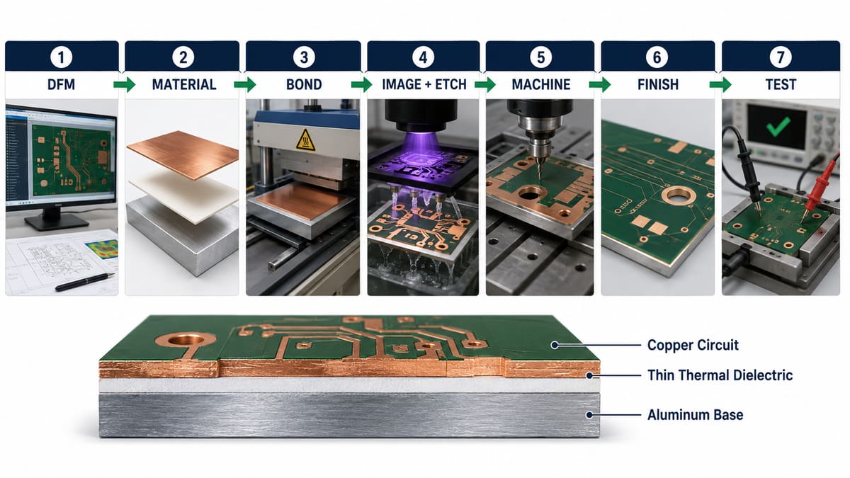
The aluminum PCB manufacturing process converts copper-clad insulated metal substrate into a patterned, protected and tested circuit board while preserving adhesion, electrical isolation and a low-resistance heat path. A typical single-sided stack has a copper circuit layer, thermally conductive dielectric and aluminum base. More complex constructions may require additional isolation or multilayer bonding and must be agreed with the fabricator rather than assumed from the single-sided route.
How Does the Aluminum PCB Manufacturing Process Work?
The process is continuous: every step must protect the dielectric-to-metal interface and finished aluminum surface while forming the copper circuit accurately.
1. Engineering Review and DFM Analysis. CAM engineers verify outline, copper features, hole types, keep-outs, polarity markings and whether any hole or slot can expose the conductive metal base. An ambiguous plated-hole request can create an isolation risk or force a different construction, so the buyer should receive clarified stackup and hole notes before release.
2. Stack-Up and Material Selection. The copper, dielectric and aluminum base are selected as a system. The dielectric must conduct heat while meeting electrical isolation and bonding needs; choosing only the highest advertised thermal conductivity can sacrifice other requirements. The approved material designation or performance specification should be recorded for repeat orders.
3. Panel Cutting and Surface Preparation. IMS sheets are cut to working size, inspected for scratches and flatness, cleaned and handled to prevent contamination. Oils, oxide or embedded debris at a bonding surface can promote voids or delamination. Incoming inspection and material lot traceability are the relevant buyer evidence.
4. Dielectric Bonding or Laminate Preparation. Depending on the supplied IMS material and board construction, the thermally conductive dielectric and copper are bonded to the aluminum under a controlled material-specific cycle. Temperature, pressure, cleanliness and resin flow affect adhesion, thickness and voiding. A poor interface raises both thermal resistance and reliability risk even when the circuit passes continuity.
5. Circuit Imaging. Photoresist and artwork transfer define pads and traces on the copper surface. Registration, exposure and resist adhesion matter because the circuit is later etched; missing resist can remove wanted copper, while residual resist can leave shorts. First-panel imaging checks prevent repeating the error across a lot.
6. Copper Etching and Inspection. Unprotected copper is removed to form the circuit. Copper thickness, chemistry and dwell time control undercut and finished conductor geometry. AOI or verified visual inspection should identify opens, shorts, edge damage and incomplete etch before mask hides the copper.
7. Drilling, Routing and Deburring. Mounting holes, slots and outlines are machined with tooling suitable for the metal base. Tool wear, feed, support and cutting direction affect burrs, smear, dimensional accuracy and flatness. Burrs can interfere with heatsink contact or damage insulation, so hole/outline inspection and a controlled deburring step are essential.
8. Solder Mask, Legend and Surface Finish. Solder mask protects the copper and controls exposed pads; legend identifies polarity and assembly locations. The selected surface finish protects solderable areas. Mask registration, cure, pad cleanliness and compatibility with the assembly process are checked rather than treating a white LED-board mask as purely cosmetic.
9. Electrical, Dimensional and Insulation Testing. Electrical test checks opens and shorts in the copper circuit. Dimensions, warpage, hole position and edge quality are inspected against the drawing. Where the project requires isolation or thermal evidence, the test method and acceptance values must be defined in the purchase specification; they cannot be inferred from the words “aluminum PCB.”
10. Final Inspection, Packaging and Release. Finished boards are reviewed for contamination, scratches, exposed metal, mask defects, burrs and identification. Packaging protects the finish and metal surface in shipment. Lot, material and test records should remain linked to the released boards.
What Materials Are Used in Aluminum PCB Manufacturing?
The core material decision is the combination of copper circuit, thermally conductive dielectric and aluminum base. These layers must be evaluated together because a thin dielectric may improve heat transfer but still has to meet voltage, manufacturing and reliability requirements.
| Layer | Main function | Engineering decision | Risk if poorly specified |
| Copper foil | Carries current and forms pads | Finished copper and feature geometry | Excess temperature rise, etch undercut or poor solder joints |
| Thermal dielectric | Transfers heat while isolating copper | Thermal resistance, thickness, isolation and adhesion | Hot spots, breakdown, voids or delamination |
| Aluminum base | Spreads heat and provides stiffness | Thickness, alloy/condition, flatness and finish | Machining burrs, poor heatsink contact or distortion |
| Solder mask/finish | Protects copper and supports assembly | Color, cure, pad finish and process compatibility | Misregistration, contamination or solderability loss |
How Is an Aluminum PCB Stack-Up Designed?
Start at the component junction and trace the entire thermal path through pad, copper, dielectric, aluminum base, thermal interface material and heatsink or chassis. The metal base is not automatically ground, and mounting hardware must not compromise isolation. Clearly identify metal-exposed holes, insulated holes, non-plated mounting holes and any required chassis connection.
For multilayer or plated-hole concepts, ask the manufacturer to confirm the actual build method and keep-out rules. Do not place a conventional FR-4 via through the metal base and assume normal hole-wall plating will provide safe isolation.
What Are the Key Manufacturing Challenges?
| Challenge | Failure signal | Factory check | Buyer evidence |
| Dielectric bond quality | Voids, lifting or thermal drift | Material/cycle control and interface inspection | Approved construction and lot traceability |
| Circuit etching | Narrowed traces, shorts or opens | Etch compensation and AOI | Finished copper requirement and electrical test |
| Metal machining | Burrs, smear, distortion or poor fit | Tool-life control and dimensional inspection | Hole/outline report or first-article measurement |
| Electrical isolation | Leakage or short to base | Construction review and specified test | Test method and acceptance requirement |
| Flatness/contact | Uneven heatsink interface | Handling and warpage inspection | Drawing tolerance and assembly-fit check |
How Does Design Affect Thermal and Electrical Reliability?
Component placement and copper spreading determine where heat enters the IMS structure. Concentrating power on small pads, interrupting the heat-spreading copper or creating an uneven mechanical clamp can leave local hot spots even when the material datasheet looks strong. Thermal simulation or measurement should include the full assembly boundary conditions, not only the laminate value.
Electrical reliability depends on clearance from exposed aluminum edges and machined features, dielectric integrity and mounting isolation. Include edge and hole keep-outs in the design rules and inspect the final mechanical stack with screws, washers, thermal interface material and heatsink.
What Tests Ensure Aluminum PCB Quality?
Testing must match the risk. Electrical continuity alone cannot prove thermal performance or insulation integrity.
| Test or inspection | What it checks | When to request |
| Electrical test | Copper opens and shorts | Every released fabrication lot |
| Visual/AOI | Etch, mask and surface defects | Routine process control |
| Dimensional/flatness inspection | Outline, holes, burrs and heatsink contact geometry | Mechanically constrained assemblies |
| Isolation test | Electrical separation from metal base | When defined by voltage and product requirements |
| Thermal characterization | Performance of a defined coupon or assembly path | Thermally critical validation with an agreed method |
| Cross-section or bond evaluation | Construction and interface condition | Qualification, failure analysis or special acceptance plans |
How Long Does Aluminum PCB Manufacturing Take?
Lead time depends on whether the selected IMS laminate is stocked, the complexity of holes/slots, surface finish, required testing, tooling and order quantity. Prototype schedules can lengthen when a custom dielectric, unusual base thickness or qualification evidence is required. Ask for a schedule only after the construction and acceptance plan are frozen.
How Do You Choose a Reliable Aluminum PCB Manufacturer?
Look for an engineering answer to the proposed stackup, not a generic aluminum-board capability statement. Ask how the dielectric construction is controlled, how holes through or near the metal base are handled, how burrs and flatness are inspected, what substitution rules apply and which tests can be linked to the lot.
A reliable supplier should also explain which values come from the laminate supplier, which are controlled during fabrication and which require assembly-level validation. This prevents a material datasheet number from being mistaken for the finished system result.
What Should Be Included in an Aluminum PCB RFQ?
- Gerber/ODB++ data, drill files and fabrication drawing
- Layer structure, finished thickness and copper requirement
- IMS material designation or required thermal/electrical performance
- Aluminum base thickness, exposed-metal areas and surface condition
- Hole/slot plating and isolation definitions
- Outline, flatness and heatsink-interface tolerances
- Solder mask color, legend and surface finish
- Electrical, isolation, dimensional or thermal test requirements
- Prototype and production quantity plus report/traceability needs
Frequently Asked Questions
Is an aluminum PCB the same as a metal-core PCB?
An aluminum PCB is a common type of metal-core or insulated-metal-substrate PCB. Metal-core constructions may also use other metals, so the exact base and dielectric must be specified.
Can aluminum PCBs have plated through-holes?
Some specialized constructions can support isolated or plated features, but they do not follow the simplest single-sided IMS route. Confirm the stackup, isolation method and design rules with the fabricator before layout release.
What controls the thermal performance most?
The full heat path controls performance. Dielectric thermal resistance, copper spreading, base thickness, interface material, clamping and heatsink conditions all matter.
Why can an aluminum PCB delaminate?
Contamination, poor surface preparation, voids, an unsuitable bond cycle, material mismatch or thermal/mechanical stress can weaken the interface. Cause confirmation may require cross-section and process records.
Are all mounting holes connected to the aluminum base?
No. A hole may expose the base, require electrical isolation or be designed as a deliberate chassis connection. The drawing must state the intended condition.
Which surface finish is used on aluminum PCBs?
Several finishes may be available depending on pad geometry, assembly and storage requirements. Choose the finish for solderability and product needs, not simply because it is common on FR-4.
Can a normal PCB electrical test verify heat dissipation?
No. Electrical test finds circuit opens and shorts. Thermal performance needs a defined coupon or assembly-level method with known boundary conditions.
What files are needed for a quotation?
Provide fabrication data, drill files, drawing, stackup/material requirement, mechanical tolerances, surface finish, quantities and acceptance tests. Add assembly/heatsink information when it changes the thermal or mounting review.
Request an Aluminum PCB Manufacturing Review
Send your Gerber or ODB++ files, fabrication drawing, IMS construction, copper/base requirements, hole isolation notes and test expectations through the PCBTRY contact page. An engineering review before quotation can identify dielectric, metal-edge, machining and heatsink-interface risks while they are still inexpensive to correct.



0 Comments