




The CCTV PCB manufacturing process combines bare-board fabrication, component assembly, firmware loading and camera-specific functional testing. A board can pass continuity and AOI yet still produce noisy, unstable or poorly aligned video, so manufacturing controls must cover power integrity, high-speed interfaces, image-sensor handling, optics, infrared operation and enclosure integration.
PCBTRY can review Gerber data, BOM, CPL, drawings, firmware and test requirements before quotation. Send the intended sensor, lens/module interface, power architecture, video interface and environmental conditions so DFM and test coverage can be planned before production.
What Is the CCTV PCB Manufacturing Process?
It is the controlled route from released camera electronics data to a tested PCB or PCBA used in an analog, IP, PoE, infrared or smart surveillance camera. The exact route depends on whether the PCB carries the image sensor, accepts a separate camera module, drives IR LEDs, processes video or manages network and power functions.
What Files and Requirements Must Be Reviewed First?
| Input | Controls | Risk if missing |
| Gerber/ODB++ and stackup | PCB geometry and signal structure | Wrong impedance or mechanical fit |
| BOM and approved parts | Sensor, processor, memory and power devices | Package or performance mismatch |
| CPL and assembly drawing | Placement, polarity and module orientation | Repeated assembly error |
| Firmware and programming note | Hardware/software revision | Functional result cannot be reproduced |
| Image-test specification | Scene, lighting, limits and records | Electrical pass hides image defects |
| Mechanical/optical data | Lens, sensor and housing relationship | Focus, light leak or alignment failure |
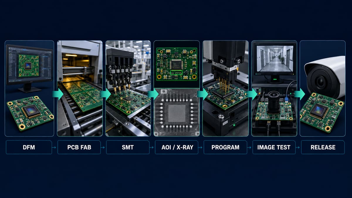
How Does the CCTV PCB Manufacturing Process Work?
1. DFM and system review. Engineers reconcile PCB, assembly, firmware, optics and test data. Power rails, sensor clock, high-speed video lanes, Ethernet/PoE, IR drivers, connector loads and test access are reviewed as one system.
2. Stackup and material preparation. The board shop selects the approved laminate, copper and finish and confirms controlled structures where specified. Material substitutions require review because dielectric and copper changes can affect loss, impedance and thermal behavior.
3. Imaging, drilling, plating and etching. Copper patterns and plated holes are created, aligned and inspected. Opens, shorts, plating defects or registration errors can interrupt sensor data, power or shielding.
4. Solder mask, legend and surface finish. Mask openings and finish must suit fine-pitch assembly and inspection. Contamination or damaged sensor-area surfaces create downstream yield and image-quality risk.
5. Electrical test and bare-board release. Flying-probe or fixture testing checks PCB opens and shorts against the released netlist. It does not verify camera function.
6. Material control and SMT setup. Component identity, moisture handling, feeder setup, stencil and programs are verified. Image sensors and optical modules need handling and cleanliness controls appropriate to the product.
7. Paste printing, SPI, placement and reflow. Paste deposits are inspected, components are placed and a measured profile forms the solder joints. Fine-pitch processors, memory, sensor interfaces and bottom-terminated packages demand controlled inspection coverage.
8. AOI and selective X-ray. AOI checks visible polarity, placement and joints; X-ray examines selected hidden joints. Neither detects every electrical or imaging fault.
9. Programming and electrical test. Firmware revision, boot, current draw, rails, communications and interfaces are verified with controlled fixtures and limits.
10. Camera and system testing. The assembled camera is tested with the intended sensor/lens path, lighting modes and interfaces. Image stability, noise, focus, frame delivery, IR switching, restart and thermal behavior are checked as specified.
Which Design Choices Most Affect CCTV PCB Quality?
Power noise, reference-plane continuity, sensor clock coupling, high-speed routing, decoupling, thermal paths and connector placement can appear directly in the video output. Keep switching regulators and IR LED current loops away from sensitive sensor supplies and clocks, then verify the finished design under real operating modes rather than relying on layout appearance.
What Manufacturing Challenges Cause Camera Failures?
| Symptom | Possible cause | Useful check |
| Image noise or bands | Rail noise, clock coupling, grounding or IR driver interaction | Power measurement plus controlled image test |
| No video/intermittent frames | Interface joint, impedance, connector or firmware issue | Link logs, electrical inspection and known-good module |
| Blur/focus variation | Sensor/lens position or housing tolerance | Optical fixture and focus target |
| Night-mode defect | IR leakage, switching noise or thermal drift | Dark-scene and IR-on test |
| Boot loop | Power sequencing, inrush, firmware or component fault | Rail/current capture and reset log |
What Tests Ensure CCTV PCB Quality?
Use bare-board electrical test, SPI/AOI, selective X-ray, rail/current measurements, programming verification, interface checks and functional image tests. Outdoor or high-reliability products may also need product-defined temperature, humidity, ingress, vibration or run-in validation. The customer specification—not a generic checklist—sets the limits.
How Long Does CCTV PCB Manufacturing Take?
Lead time depends on component availability, stackup, tooling, firmware readiness, test fixtures, camera modules, optics and qualification. Separate PCB fabrication, PCBA, programming, image-test development and system validation on the schedule.
How Do You Choose a CCTV PCB Manufacturer?
- Ask how PCB, BOM, CPL, firmware and mechanical revisions are reconciled.
- Confirm sensor/module cleanliness and handling controls.
- Request the SPI, AOI, X-ray and functional-test coverage map.
- Define image-test scenes, lighting modes, limits and retained data.
- Check how substitutes and firmware changes are approved.
- Verify the supplier can diagnose electrical, optical and software interactions.
Frequently Asked Questions
Is electrical test enough for a CCTV PCB?
No. It can find opens, shorts or defined electrical faults but does not prove image quality, focus, IR operation or firmware behavior.
Why can a camera board pass AOI but show noisy video?
AOI sees accessible physical features. Power noise, signal integrity, optical contamination and firmware interactions require electrical and image tests.
What files are needed for quotation?
Send Gerber/ODB++, drill, drawing, stackup, BOM, CPL, assembly notes, firmware requirements, quantity and test specification.
When is X-ray needed?
Use it for selected hidden joints when package construction and risk justify it. Define coverage and acceptance criteria.
Does every CCTV board need conformal coating?
No. Coating depends on enclosure protection, environment and product specification, and it requires cleanliness, masking and cure control.
How should image quality be tested?
Use controlled scenes, lighting and lens/module setup with defined limits for the functions that matter, including IR or low-light modes when applicable.
Can the manufacturer substitute the image sensor?
Only with approval. Sensor changes can affect mechanics, power, firmware, optics and image tuning.
What should a first article include?
Include the approved data revision, assembly inspection, firmware identity, electrical readings and representative image-test results.
Request a CCTV PCB Engineering Review
Send PCBTRY your fabrication, assembly, firmware, camera-module and test information. Request an engineering review and quotation to identify PCB, PCBA and image-test risks before production.



0 Comments