




A heavy copper PCB is manufactured by building and patterning substantially more copper than a conventional board while keeping trace geometry, resin filling, hole-wall integrity and board flatness within the agreed drawing requirements. It is used for power conversion, motor drives, battery systems, industrial controls and other designs where conductors must carry current or spread heat. The extra copper changes the process window: artwork compensation, plating distribution, etching, lamination and solder-mask coverage all require more attention than on a standard thin-copper board.
PCBTRY supports PCB manufacturing with engineering review, DFM feedback and fabrication testing. For a meaningful assessment, send the Gerber files, drill data, stack-up, finished copper requirement by layer, board thickness, material requirement, current/temperature-rise targets and acceptance criteria. Engineering can then evaluate the actual construction rather than quote from “heavy copper” as a label.
What Is a Heavy Copper PCB Manufacturing Process?
The heavy copper PCB manufacturing process is the controlled sequence used to create, laminate, connect and verify layers with unusually thick finished copper. The term is commonly associated with copper weights around 3 oz/ft² and above, but buyers should specify the required finished copper thickness and tolerance instead of relying on the category name. Different factories and designs may use different starting foils, plating build-up and etch compensation.
Thicker copper is useful only when the conductor shape, via structure, thermal interfaces and assembly process support the electrical goal. A nominal copper weight alone does not prove current capacity or temperature rise.
How Does the Heavy Copper PCB Manufacturing Process Work?
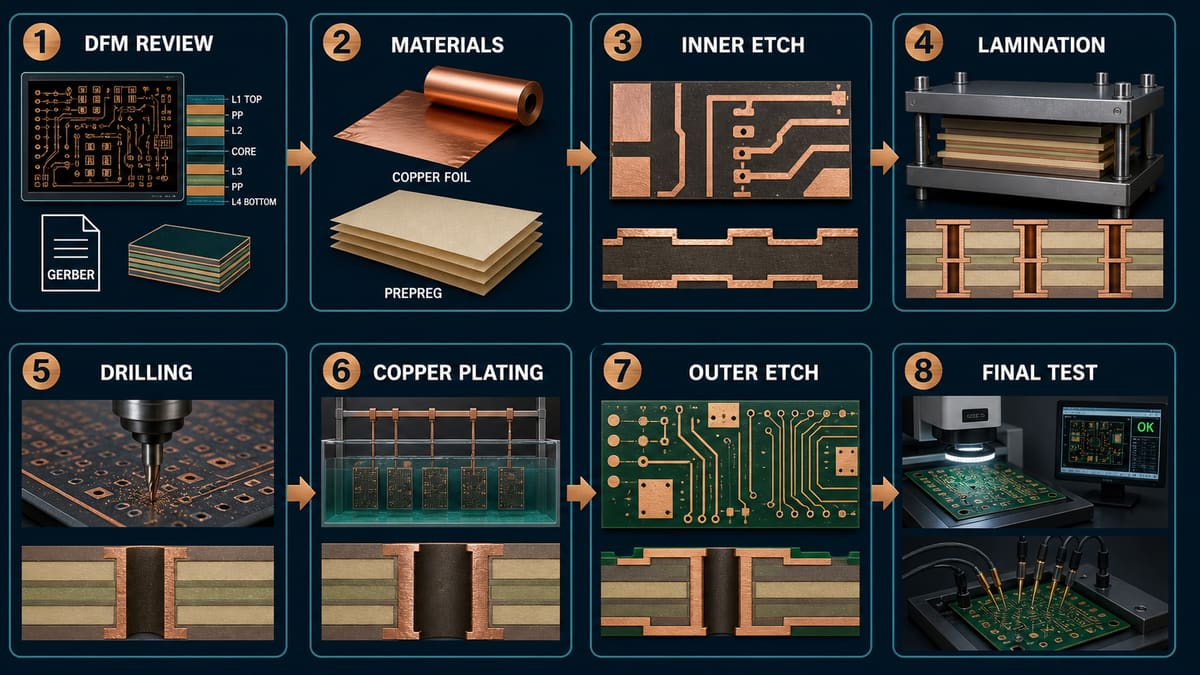
The process starts with engineering review and finishes with inspection and electrical release. The exact route depends on layer count, finished copper, feature geometry, material and reliability class, but the control logic remains consistent.
1. Engineering Review and DFM Analysis
CAM engineering checks the requested finished copper by layer, trace and space geometry, pad and annular-ring allowance, copper balance, drill structure, board outline and test requirements. This is where a design based on thin-copper rules must be corrected. If the available etch compensation cannot preserve the required conductor, a prototype may look acceptable while the production distribution does not.
Buyer evidence: an approved stack-up and DFM issue list that identifies finished copper, critical features and accepted deviations.
2. Stack-Up and Material Preparation
The manufacturer selects cores, prepregs and copper foils that can create the electrical and mechanical construction. Resin content and flow must be capable of filling the valleys beside tall copper features during lamination. Poor selection can leave resin-starved areas, voids or excessive thickness variation.
Buyer evidence: material designation, controlled stack-up and finished-thickness requirement tied to the drawing.
3. Inner-Layer Imaging and Etching
Photoresist defines the inner circuitry, then etching removes unwanted copper. Because etchant attacks laterally as it removes copper vertically, thick conductors can develop a trapezoidal cross-section. Artwork compensation and process control must preserve the finished conductor and isolation, not merely the top-view image.
Release check: AOI and dimensional coupon data show no opens, residual copper shorts or unacceptable conductor loss.
4. Oxide Treatment, Lay-Up and Lamination
Prepared inner layers are aligned with prepreg and copper foil, then laminated under a controlled heat and pressure cycle. Resin must fill around thick copper without trapping voids, while the stack stays registered and balanced. Excessive or insufficient flow can change dielectric spacing, finished thickness and flatness.
Release check: registration, thickness, void risk and warpage are within the project specification.
5. Drilling, Desmear and Hole Preparation
Drilling creates the via and component-hole geometry. Heavy copper increases thermal and mechanical load around the drill interface, while multilayer registration still controls breakout risk. Hole cleaning and desmear must expose clean copper for the next metallization step; debris or damaged resin can weaken the connection.
Buyer evidence: drill controls and representative microsection results for critical plated structures.
6. Electroless Copper and Pattern Plating
A conductive seed layer is deposited in the holes, followed by electrolytic copper build-up on hole walls and selected outer-layer features. Current distribution, panel pattern and plating area influence thickness uniformity. Simply increasing plating time does not guarantee equal copper in dense and open areas.
Release check: coupon or microsection measurements demonstrate the specified finished surface and hole copper at agreed locations.
7. Outer-Layer Etching, Solder Mask and Surface Finish
After plating and resist processing, exposed base copper is etched away to isolate the outer circuits. Thick copper edges create greater topography, so solder mask must cover conductor shoulders and avoid thin spots or trapped contamination. The selected surface finish then protects exposed pads and supports the intended assembly process.
Failure risk: residual copper can create shorts; inadequate mask coverage can expose conductor edges; an unsuitable finish can complicate soldering.
8. Profiling, Inspection and Electrical Testing
The board is routed or scored, cleaned and inspected. AOI, visual/dimensional inspection, electrical testing and representative microsections verify different failure modes; no single test replaces the others. Additional thermal or reliability validation must be defined by the application and purchase specification.
Release evidence: electrical-test status, inspection record, dimensional results and any specified coupon or reliability report.
What Materials Are Used in Heavy Copper PCBs?
Material selection must match temperature, electrical, mechanical and assembly conditions as well as the copper construction. Standard epoxy-glass systems may suit many industrial power boards, while higher-temperature or specialized materials may be needed for demanding operating or assembly profiles. The correct choice depends on the approved datasheet and construction—not a generic “high-Tg” claim.
| Material decision | Why it matters with heavy copper | What to specify |
| Core and prepreg system | Controls resin filling, dielectric spacing and thermal/mechanical behavior | Material family, approved equivalents and stack-up |
| Resin content and flow | Must fill the spaces around tall copper features | Construction approved by engineering, not a buyer-guessed universal value |
| Copper foil and plated build-up | Affects final thickness, etch profile and surface distribution | Finished copper by layer and tolerance |
| Solder mask | Must cover pronounced copper edges without thin spots | Mask type, color where relevant and acceptance criteria |
| Surface finish | Changes pad protection, flatness and assembly compatibility | Finish tied to component and process needs |
How Is a Heavy Copper PCB Stack-Up Designed?
A workable stack-up balances copper distribution, dielectric fill, finished thickness, registration and electrical performance. Specify which layers carry heavy copper; writing one copper weight for the entire board can create ambiguity. Large differences between opposing layers or uneven copper areas can increase bow, twist and plating variation.
The designer and fabricator should agree on starting foil versus finished copper, dielectric thickness targets, resin strategy, via construction and coupon location. For controlled impedance, the field solver must use the actual finished geometry and material data; copying a thin-copper stack-up can misrepresent both conductor shape and dielectric spacing.
Why Are Plating and Etching Harder with Heavy Copper?
Plating must distribute a large copper build-up across nonuniform panel patterns, while etching must remove more copper without consuming too much conductor width. These are coupled processes: plating variation changes the amount and profile the etch process must remove.
Engineers should judge the finished cross-section, not only the nominal weight. Ask how minimum spacing, feature compensation and coupon placement are established for the actual copper requirement. If a supplier quotes a fine feature without reviewing copper thickness and panel pattern, the capability claim is incomplete.
How Does Lamination Affect Heavy Copper Reliability?
Lamination must push resin into the deep spaces between copper features while maintaining registration and a balanced final panel. Resin starvation can reduce insulation and adhesion; trapped voids can concentrate stress; excessive flow can shift thickness and registration. Dense copper next to large cleared regions makes the window harder to control.
Useful evidence includes the approved material construction, representative microsection, finished thickness and warpage results where required. A visually flat prototype is not sufficient evidence for a multilayer high-power design.
How Does Design Affect Current and Thermal Reliability?
Heavy copper reduces conductor resistance and can spread heat, but current and temperature rise still depend on finished cross-sectional area, path length, ambient conditions, cooling, via distribution and connection interfaces. Neck-downs, thermal-relief spokes, connector pads and plated holes can become bottlenecks even when the main pour is thick.
- Identify the complete current path, including terminals, vias and layer transitions.
- Model or test temperature rise under the real enclosure and cooling conditions.
- Avoid abrupt width changes and isolated thermal concentrations where possible.
- Tell the assembler about high thermal mass so the soldering profile and equipment can be validated.
What Are the Main Heavy Copper Manufacturing Challenges?
The main challenges are trace-profile control, copper distribution, resin filling, registration, hole reliability, solder-mask coverage and flatness. Each needs a matching inspection method and buyer evidence.
| Challenge | Likely defect | How it is judged | Buyer evidence |
| Etch compensation | Undersized or trapezoidal conductors; residual copper | AOI and cross-section/dimensional checks | Finished feature acceptance and coupon data |
| Plating distribution | Local copper too thin or too heavy | Thickness measurement and microsection | Specified measurement locations and results |
| Resin fill | Voids or resin starvation | Microsection and process inspection | Approved stack-up and representative section |
| Copper balance | Bow, twist or registration shift | Dimensional/flatness measurement | Drawing tolerance and inspection result |
| Hole formation | Smear, breakout or weak barrel | AOI where applicable and microsection | Hole-wall and registration evidence |
| Solder-mask coverage | Thin mask on copper shoulders or exposed edges | Visual inspection and adhesion/coverage criteria | Accepted mask criteria and first-article photos |
What Tests Ensure Heavy Copper PCB Quality?
Testing should connect the fabrication risks to the application requirements. AOI finds pattern defects, electrical test checks opens and shorts, dimensional inspection checks outline and hole geometry, and microsectioning verifies internal features such as conductor profile and plated-hole structure. Solderability, thermal cycling or other reliability tests are added only when required by the drawing, standard or qualification plan.
Ask which tests apply to every board, which use sample coupons, what acceptance document controls the result and what report will ship. “100% tested” is incomplete unless the test type and coverage are named.
How Long Does Heavy Copper PCB Manufacturing Take?
Lead time depends on material availability, copper build-up, layer count, lamination cycles, drilling, finish, test plan, panel utilization and whether DFM questions are resolved. Heavy copper may need more engineering review and process verification than a routine board, so a universal prototype or production lead time would be misleading.
For a usable schedule, submit complete data and ask the supplier to separate engineering approval, material procurement, fabrication, inspection and shipment. A rushed start with an unresolved copper definition can cost more time than the review saves.
How Do You Choose a Heavy Copper PCB Manufacturer?
Choose a manufacturer by its ability to review and prove the exact construction, not by the highest copper number on a capability page. The supplier should explain how design rules change with finished copper, how plating and etching are controlled, how resin filling is evaluated and what inspection evidence is available.
- Send the same revision-controlled RFQ package to each supplier.
- Ask for a layer-by-layer finished copper interpretation.
- Confirm minimum features against that copper, not a generic table.
- Review the proposed stack-up, resin strategy and copper balance.
- Define microsection, electrical-test and dimensional evidence.
- Confirm material substitutions require approval.
- Compare exceptions and test coverage, not only price and calendar days.
Frequently Asked Questions
What copper thickness is considered heavy copper?
Many industry references use about 3 oz/ft² and above, but definitions vary. Put the required finished copper thickness and tolerance on the drawing for every relevant layer.
Is heavy copper made only from thick copper foil?
Not always. The route may combine starting foil with electrolytic build-up. Ask the fabricator to confirm starting and finished copper so the etch and stack-up assumptions are clear.
Why do heavy copper traces have a trapezoidal profile?
Etchant removes copper laterally as well as vertically. More copper removal increases side attack, so artwork compensation and process control must protect the finished cross-section.
Can heavy copper PCBs have fine traces and spaces?
Capability becomes more constrained as copper increases. The answer depends on finished copper, feature location and the supplier’s qualified process; obtain a DFM decision for the real Gerber data.
Do heavy copper boards need special prepreg?
They need a construction with enough suitable resin flow to fill around the copper topography. The fabricator should select and document the material system rather than apply one universal prepreg rule.
How are heavy copper PCBs electrically tested?
Continuity and isolation are checked against the net data using an appropriate electrical-test method. This verifies opens and shorts but does not replace microsection, dimensional or application-level thermal validation.
What files are required for a quotation?
Send Gerbers, NC drill files, stack-up, fabrication drawing, finished copper per layer, material and finish requirements, dimensions/tolerances, quantity and test criteria. Include current and temperature-rise goals where they influence design review.
Does heavy copper automatically solve overheating?
No. It can reduce resistance and spread heat, but bottlenecks, interfaces, airflow, enclosure temperature and component losses still control the result. Validate the complete thermal path.
Get an Engineering Review Before You Release the Order
The most useful time to resolve heavy copper risk is before panelization and tooling. Send PCBTRY your Gerber and drill package, proposed stack-up, layer-by-layer finished copper, material, thickness, surface finish, current/thermal targets, quantity and required tests through the contact page. Request a DFM review and quotation that clearly lists assumptions, exceptions and release evidence.



0 Comments