




The heavy copper PCB plating process builds copper on selected circuit areas and inside drilled holes while controlling thickness distribution across a panel. It is used when power paths need more conductor cross-section or when a design combines heavy surface copper with plated interconnections. Unlike a routine thin-copper build, the plating pattern itself changes current distribution, so isolated features, dense areas, panel edges and hole centers may not deposit copper at the same rate.
PCBTRY can review Gerber files, drill data, stack-up and finished-copper requirements before fabrication. Send the required finished copper by layer, hole structure, board thickness, acceptance class and critical current/thermal information so engineering can evaluate the plating and inspection route rather than assume that one copper-weight label describes the board.
What Is the Heavy Copper PCB Plating Process?
Heavy copper plating is controlled electrodeposition used to increase conductor and hole-wall copper beyond the starting foil or initial metallization. The finished result may combine base foil, electroless copper and electrolytic build-up. Buyers should therefore specify finished copper and tolerance at defined locations, not confuse foil weight with final plated thickness.
How Does the Heavy Copper PCB Plating Process Work?
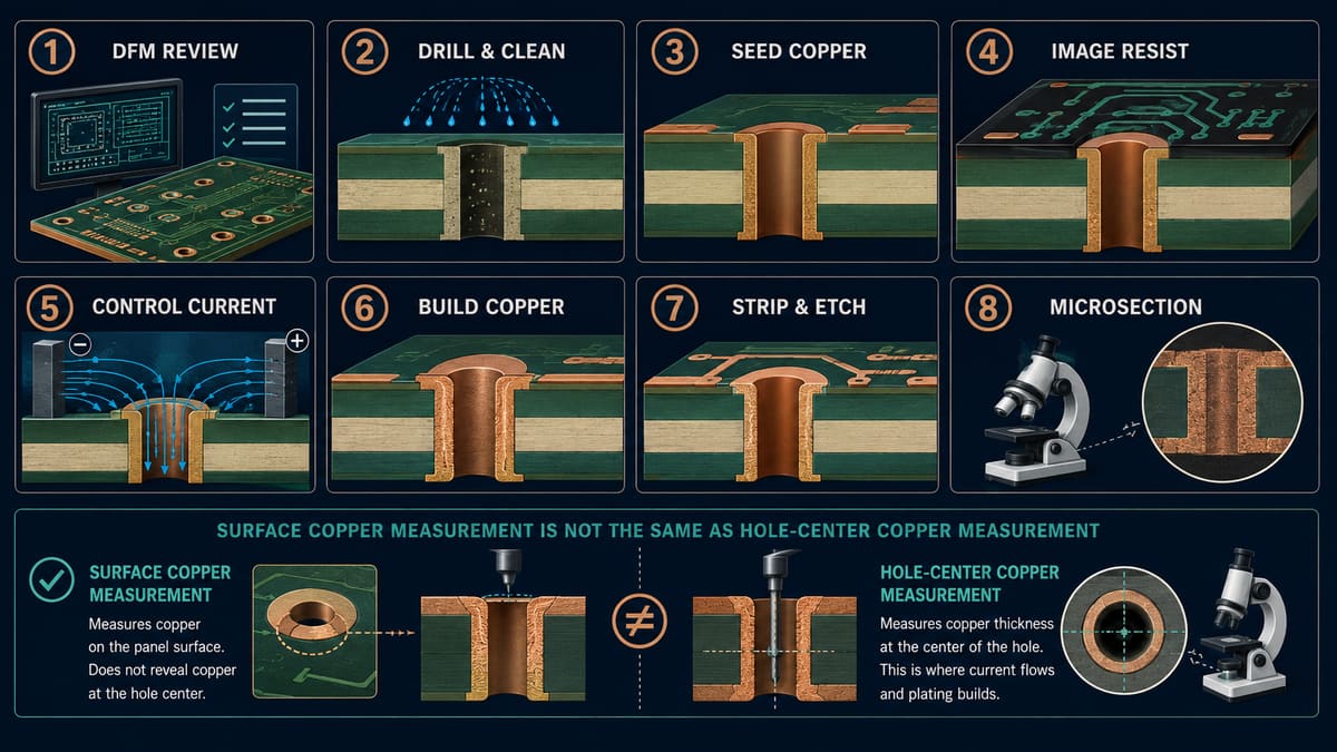
The process begins with data review and hole preparation, then creates a conductive path, plates copper under controlled conditions and verifies the deposit before later etching and finishing.
1. DFM and Finished-Copper Interpretation
CAM confirms which layers and features require heavy copper, how the finished value is measured, and whether line/space, pads, holes and panel pattern can support it. Ambiguous “3 oz board” notes can cause different assumptions for inner foil, outer finished copper and hole walls.
Evidence: approved stack-up and layer-by-layer finished-copper table.
2. Drilling and Hole-Wall Preparation
Drilling creates the interconnect geometry; cleaning and desmear expose sound internal copper and resin surfaces. Smear, debris or damaged walls can interrupt metallization and later crack under thermal stress.
Evidence: controlled drill route and representative hole preparation checks.
3. Electroless Copper Seed Layer
A thin continuous conductive layer is deposited through holes and over nonconductive surfaces so electrolytic current can reach them. Continuity and adhesion matter more here than calling the seed layer “heavy.” A discontinuity can become a void or thin barrel after build-up.
Evidence: process controls and microsection evidence where required.
4. Resist Imaging and Pattern Definition
Photoresist exposes only the features intended for pattern plating. Resist thickness and sidewall quality must accommodate the planned copper build. Poor imaging can cause nodules, bridging, distorted pads or resist entrapment.
Evidence: artwork compensation and pre-plate pattern inspection.
5. Panel Loading and Current-Distribution Control
The panel pattern, rack contact, anode arrangement, shielding, agitation and solution condition influence where current flows. Open edge features may plate faster than dense central regions. Qualified thieving or shields may redistribute current, but additions must respect electrical, high-voltage and RF constraints.
Evidence: approved tooling strategy and thickness sampling plan.
6. Electrolytic Copper Build-Up
The manufacturer controls the qualified bath, current program, temperature, agitation and time to achieve the specified deposit. Increasing time alone can overplate high-current-density areas while hole centers or dense regions remain thin.
Evidence: bath/process records and representative thickness measurements.
7. Resist Strip and Etch Handoff
After build-up and any required metallic etch resist, the temporary resist is removed and exposed base copper is etched. Excessive or nonuniform plating changes the etch burden and finished conductor profile, so plating and etching cannot be reviewed as unrelated steps.
Evidence: AOI/dimensional checks tied to finished features.
8. Thickness, Microsection and Electrical Release
Surface measurement, plated-hole microsections, visual inspection and electrical test verify different risks. A surface reading does not prove hole-center copper, and continuity alone does not prove adequate thickness or deposit quality.
Evidence: named test method, coupon location, acceptance criteria and retained report.
What Is the Difference Between Panel Plating and Pattern Plating?
Panel plating deposits copper broadly before circuit definition, while pattern plating builds copper mainly on exposed circuit features after resist imaging. The selected route affects distribution, etch burden, resist requirements and finished geometry; neither route is automatically best for every heavy-copper design.
| Decision | Panel plating | Pattern plating |
| Where copper grows | Broad panel surface and holes | Exposed circuitry and holes |
| Main control concern | Panel uniformity and later imaging/etching | Pattern-dependent current density and resist capacity |
| Heavy-copper consequence | More copper may need patterning/etch removal | Dense and isolated features may build differently |
| Buyer action | Approve the proposed route against finished geometry and inspection evidence | |
Why Is Plating Uniformity Difficult?
Electric current and copper-ion transport are not uniform across arbitrary artwork. Panel edges, isolated pads and areas nearer effective anode/current paths can receive more deposition; dense patterns and hole centers may receive less. Throwing power describes how effectively a process deposits copper into recessed features compared with accessible surfaces, but the reported ratio is meaningful only when its measurement method and geometry are defined.
Do not accept a single surface measurement as proof of the whole panel. Agree on measurement locations that represent dense/open areas, edges/centers and critical hole structures.
How Are Plated Through-Holes Controlled?
Hole plating must remain continuous and sufficiently robust from entry to center while connecting cleanly to internal pads. Board thickness, finished hole diameter, drilling quality, desmear, seed coverage, solution movement and current distribution all influence the result. High aspect ratio increases the difficulty of transporting ions and controlling deposit thickness inside the barrel.
Representative coupons should match critical geometry. A microsection can reveal thin centers, voids, folds, separation, roughness and registration conditions that a top-surface gauge cannot see.
How Does PCB Design Affect Copper Plating?
Artwork determines the electrical load placed on the plating process. Abrupt changes from solid copper to sparse isolated features, asymmetric copper distribution, very small annular rings and mixed hole geometries increase variation or reduce inspection margin. Designers should flag areas where added thieving is prohibited because of creepage, RF or functional constraints.
- Specify finished copper by layer and critical location.
- Provide copper-balanced artwork where electrical function permits.
- Set pad and annular-ring geometry using the fabricator’s reviewed process.
- Identify controlled-impedance, high-voltage and sensitive RF areas before permitting tooling copper.
- Place or approve representative coupons for critical plated features.
What Defects Can Occur During Heavy Copper Plating?
Common risks include thickness variation, thin hole centers, voids, nodules, rough deposits, resist bridging and poor adhesion. Each needs a matching detection method.
| Defect | Possible process cause | Detection | Buyer evidence |
| Surface thickness variation | Pattern/current distribution or contact differences | Mapped thickness measurements | Locations, tolerance and results |
| Thin hole center | Limited throwing power or transport | Representative microsection | Coupon geometry and section report |
| Void/discontinuity | Poor cleaning or seed coverage | Microsection and electrical test | Section plus net test status |
| Nodule/bridge | Contamination, resist damage or local overplating | Visual/AOI and dimensional inspection | Accepted finished-feature result |
| Rough or brittle deposit | Bath/additive/process condition outside qualified window | Surface and section evaluation; specified reliability test | Process control and required qualification evidence |
| Separation at interfaces | Preparation or adhesion failure | Microsection/thermal test when specified | Acceptance standard and report |
What Tests Verify Heavy Copper Plating Quality?
A defensible test plan combines surface thickness measurement, microsectioning, visual/AOI inspection, dimensional verification and electrical test. Thermal stress, solderability or other reliability testing belongs in the plan when the drawing, applicable standard or end-use qualification requires it.
Ask what is tested on every board, what is coupon-based, where measurements are taken, what sampling applies and which document defines acceptance. “100% electrically tested” proves net continuity/isolation—not copper thickness everywhere.
How Does Plating Affect Cost and Lead Time?
Cost and schedule depend on finished copper, plated area, layer/hole construction, material, panel utilization, process cycles, coupon requirements and test reporting. Extra build-up may reduce throughput or require additional verification, but there is no honest universal lead-time multiplier.
A complete RFQ reduces delay: send Gerbers, NC drill files, stack-up, finished copper by layer, board thickness, material/finish, quantity, class/acceptance criteria, critical hole geometry and required reports.
How Do You Audit a Heavy Copper Plating Supplier?
Audit whether the supplier can interpret, control and prove your construction. Ask how it distinguishes foil from finished copper, handles pattern density, selects coupons, measures surface and hole copper, controls bath condition and links exceptions to engineering approval.
- Confirm the layer-by-layer copper interpretation in writing.
- Review the proposed panel/pattern plating route.
- Identify measurement and microsection locations.
- Define hole geometry represented by coupons.
- Specify electrical and any thermal/reliability testing.
- Require approval for material or construction changes.
- Compare evidence and exceptions—not only maximum advertised copper weight.
Frequently Asked Questions
Is finished copper the same as starting foil?
No. Finished copper may include foil plus deposited copper. Specify the final requirement by layer and confirm how the supplier interprets and measures it.
What is throwing power in PCB plating?
It describes how well a plating process deposits copper in recessed features such as hole centers relative to accessible surfaces. Compare values only when geometry and measurement method are defined.
Why do panel edges plate more heavily?
Electric-field and current-density distribution can concentrate deposition at exposed edges or isolated features. Tooling, shields, thieving and qualified process controls are used to redistribute it.
Can electrical test verify hole copper thickness?
No. It detects opens and shorts at test conditions, but a continuous thin barrel may still pass. Microsection or another specified thickness method is needed.
Does longer plating always create better heavy copper?
No. It can overplate high-current-density areas while less accessible locations remain comparatively thin. Uniformity and deposit quality matter with total build.
Can a manufacturer add copper thieving automatically?
Only within agreed constraints. Thieving can help distribution but may affect high-voltage spacing, RF behavior or customer-controlled artwork; define approval rules.
What files are needed for review?
Send Gerbers, drill data, stack-up, fabrication drawing, finished copper per layer, thickness, material, finish, quantity and acceptance/test requirements.
Which report should I request?
Request the evidence relevant to risk: layer/finished-copper confirmation, mapped measurements, representative microsections, electrical-test status and any specified qualification results.
Request a Plating-Focused DFM Review
Send PCBTRY the Gerber and drill package, proposed stack-up, finished copper per layer, critical hole dimensions, material, finish, quantity and acceptance criteria through the contact page. Ask engineering to identify plating-distribution risks, coupon locations and release evidence before tooling.



0 Comments